

FPGAs used to be mysterious, expensive devices, but these days you can buy surprisingly capable boards for very little money. Some years ago, I did an FPGA Bootcamp over on Hackaday.io. Much of that material still applies, but the hardware is dated. So I decided it was time to update it, using the inexpensive Tang Nano 20K and its GOWIN GW2AR-18 FPGA as the main platform, with perhaps a few excursions into other FPGAs.
History and Motivation
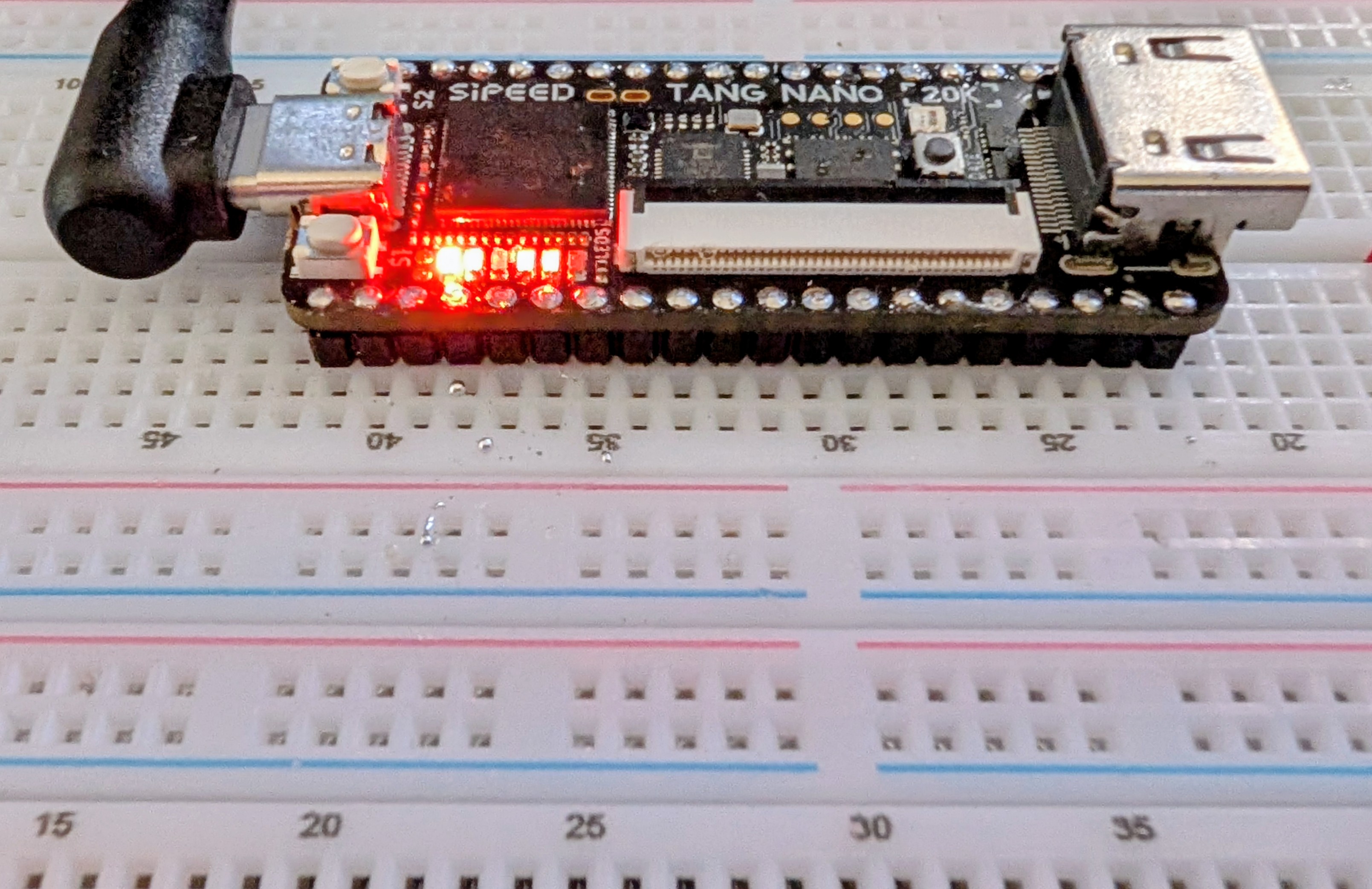 Once upon a time, if you wanted to have a custom IC, you went with a wheelbarrow full of money to a semiconductor company. However, some smart person at a semiconductor fab eventually realized they could make a chip with a lot of uncommitted blocks on it and then, for a custom chip, only design the wiring that connected them together. This still required a wheelbarrow full of money, but it was a smaller wheelbarrow.
Then one day, someone realized they could do the same thing but make the electrical connections between the blocks configurable. Maybe have fuses you can blow, or use EEPROM or RAM cells to remember which blocks are connected to which. It is complicated, sure, but then you can make many of these chips and sell them to people who could, in theory, make their own custom chips without your help.
When do you need an FPGA? A classic classroom exercise for an FPGA, for example, is a traffic light because it shows off how to do state machines, which are important for some kinds of FPGA designs. But other than as a learning example, why would you do this? Even a simple 8-bit CPU can handle a traffic light.
Suppose instead that you have hundreds of digital sensors on a rocket, and any one of them must raise an alarm within a few microseconds. A processor has to sample inputs in groups, service interrupts, or rely on extra hardware. An FPGA can simply implement the equivalent of one enormous OR gate. It watches every input continuously, and unrelated logic elsewhere in the FPGA does not steal execution time from it. Can you do it with a microcontroller? Probably, but not easily. For some classes of problems, an FPGA is the better answer.
Of course, you can also build a CPU on your FPGA and some FPGAs have CPUs in the same package. This is often a sweet spot because then things that are easy to do in software, you do in software. Things that are easier to do in hardware, you do in the FPGA.
The 20K Solution
How big of an FPGA do you need? It is hard to compare FPGAs because the blocks are different. Think of PC memory. You can talk about 1 GB vs 4 GB, but the full picture depends on the memory speed, bandwidth, and timing. FPGAs are the same way. Two FPGAs may have a similar number of building blocks, but one may have much more powerful building blocks than the other. However, the 20K board’s FPGA is quite capable, even if it is hard to compare it directly to other FPGAs from other vendors.
It uses GOWIN’s GW2AR-LV18QN88C8/I7, which contains 20,736 four-input look-up tables (LUT4s) and 15,552 flip-flops. The exact maximum clock rate depends heavily on the logic and routing, so there is no single useful “FPGA clock speed,” but the device is quite comfortable in the low hundreds of MHz for appropriately pipelined designs.
Where the chip shines is memory. Most FPGAs have distributed RAM, which eats up resources on the chip, and block RAM, which are dedicated RAM cells. The GOWIN has both of these options. It also has a separate 8 Mbyte, 32-bit SDR SDRAM right in the package. Of course, you have to eat up some FPGA resources to talk to it, but not as much as you might think, and certainly not as much as it would take to place an 8 Mbyte RAM in the FPGA fabric.
There are other special-purpose blocks, like 48 18×18 multipliers, you can configure in a few ways. The Nano 20K board also has a programmable clock generator, QSPI flash (64 Mbits), and connections for audio, LCD, microSD, and HDMI. A microcontroller lets you program the clock generator, flash the chip via JTAG, or provide a virtual serial port back to the host.
Simply FPGA
The basic workflow for an FPGA is:
- Define the logic you want using an HDL (we will use Verilog, but VHDL is also common).
-
Define a “top block” that connects to the outside world.
-
Set up constraints that mainly tell the device which pins connect to which ports on the top block.
-
Run a synthesis process that converts your HDL to primitives.
-
Run a place and route process that assigns primitives to specific chip resources and produces a “bitstream.”
-
Download the resulting bitstream to the FPGA’s RAM or to the configuration flash (which makes it survive a power cycle).
You can do all of these things with GOWIN’s IDE or open-source tools that we’ll talk about later.
Inside
You might think you just want to draw schematics. Some FPGA tools allow that, but the GOWIN IDE does not. It can, however, draw schematics to show you what you asked for. Turns out, if you are doing something large, schematics are a pain. Why draw out a 7-segment decoder when you can just describe it using a software-like language?
Inside the chip, there aren’t really uncommitted gates per se. There are lookup tables. So if you specify that Z=A|(BC)|(A^D) it doesn’t really go find an AND gate, an OR gate and an XOR gate. It just develops a table and programs that table to produce that function. That’s why LUTs — Look Up Tables — are important.
Simplicity
So let’s look at the simplest possible thing you might do.
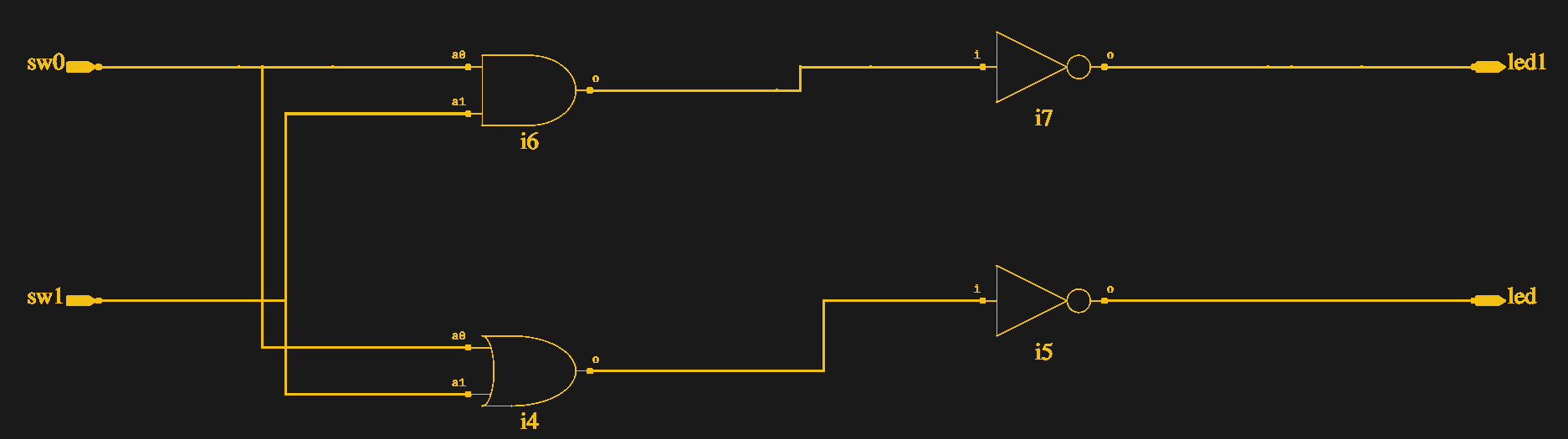
module top(output led1, output led, input sw0, input sw1);
assign led=~(sw0|sw1);
assign led1=~(sw0&sw1);
endmodule
We’ll talk more about Verilog later, but for now note that nothing “executes” these lines one at a time. This literally tells the FPGA design software to connect the two switches to a logic gate and then invert the result and connect it to the LED. At run time, this isn’t code, it is wiring.
The LEDs on the board are active low, so this just takes two inputs (presumably switches), computes the OR and AND, and outputs them to the LEDs. The switches on the 20K are pulled down so there’s no need for a pull up or pull down in the FPGA. The output is a logic one when you press the swtich.
 How do you connect the devices to your “code?” You need a constraint file, and that’s easiest done through the “Floorplan” editor (see the figure). It builds a file which you can change if you prefer to work with a file:
IO_LOC "led" 15;
IO_PORT "led" IO_TYPE=LVCMOS33 PULL_MODE=UP DRIVE=8 BANK_VCCIO=3.3;
IO_LOC "led1" 16;
IO_PORT "led1" IO_TYPE=LVCMOS33 PULL_MODE=UP DRIVE=8 BANK_VCCIO=3.3;
IO_LOC "sw1" 88;
IO_PORT "sw1" IO_TYPE=LVCMOS33 PULL_MODE=NONE BANK_VCCIO=3.3;
IO_LOC "sw0" 87;
IO_PORT "sw0" IO_TYPE=LVCMOS33 PULL_MODE=NONE BANK_VCCIO=3.3;
That’s it. The schematics come in two flavors. One shows what you’d expect (see the figure). The other shows opaque LUT boxes.
The video below walks through the design from starting the project to watching it work on a breadboard.
Installing
I’m glossing over a lot of details. While the GOWIN software runs on Linux, I had to do a lot to get it to work. Since I wasn’t on a supported distro, I had to work out the dependencies myself, but that wasn’t too hard.
The problem was when I tried to execute the program. The first problem was with libfreetype.so.6. I removed the private copy and linked it to my system copy. That got me a little further. However, to get it all running, I needed to set (or add) GOWIN’s lib directory to LD_LIBRARY_PATH to prevent it from picking up system libraries.
The programmer also needed a little work to not run afoul of other drivers on the system. The specific cure there for me was to build the file: /etc/udev/rules.d/99-tang-nano-20k.rules with these lines:
SUBSYSTEM=="usb", DRIVER=="ftdi_sio", ATTRS{idVendor}=="0403", ATTRS{idProduct}=="6010", ATTR{bInterfaceNumber}=="00", RUN+="/bin/sh -c 'echo $kernel > /sys/bus/usb/drivers/ftdi_sio/unbind'"
Of course, my fixes may or may not help your problems. If you are lucky, you won’t need any fixes at all. The open-source tools are perhaps a little easier to deal with, and we’ll look at those too. However, some of the GOWIN tools are nice, and you can check an option to have it always use your choice of external editors, which is a nice feature.
Next Time
If you need a refresher on digital logic, the original FPGA Bootcamp 0 lets you learn about logic design using a free tool in your browser. No FPGA required at all. Meanwhile, we’ll be looking later at open-source tools, IP, synchronous logic, and using the built-in logic analyzer, among other things. If you want to talk about this series, drop by our Discord server.
When you finish up your next FPGA project, don’t forget to send us a tip. You might see your project on Hackaday.












Sandbox and watchdog would be a good niche.
Nice! I had a look to the Open Source tools a while ago (maybe more than a year?) and many features were still not supported, but things might have changed since then! I’ll make sure I read carefully next article dealing with OSS tools!
Had a project recently and needed a ton of input/outputs. Found a really fun board for $400. TS-7800-V2 Dual Core 1.3 GHz Arm® Cortex®-A9 20k LUT Cyclone FPGA (145 Various I/O Pins)
This isn’t using a FPGA so totally unrelated to this article
Really? because I actually BOUGHT AND USED the board….
and the TS-7800-V2 board definitely has an Altera / Intel Cyclone IV FPGA….so YEAH….pretty related to this article.
Sir, this is a Wendy’s.
Except the last word was FPGA
I used a TS-7800 around 2008 or so… I’m surprised they’re still around. And yes, folks, they use an FPGA to manage their I/O.
TS-7800-V2 was released in 2018 they pretty much updated and upgraded everything. One of the guys I worked with had used a ts-7800 previously, he is the one that recommended it and was pretty impressed with the upgraded V2.
Would be nice to see a primer on programming those chips with full open-source software suite, namely Yosys, Apicula, OpenFPGALoader
Turns out there is a lot of glue required because there are a lot of moving parts. I started to put something together for myself here, which may or may not be of use if you want to see what’s in a workflow: https://github.com/pete-restall/fpga-sv-template
Still a work in progress but builds for the Tang Primer 20k, iCESugar, iCEStick and Artix7 boards I have. Uses GNU Make, Yosys, Icarus, nextpnr. Runs testbenches and formal verification. Builds an mdBook from Markdown and wavedrom. Also builds it all in GitHub actions so you can see what’s required to get a local toolchain running.
This is cool, although I predict you’ll be interested in the next installment.
I’m really keen to see a good robust FOSS FPGA toolchain come out. IMO, the biggest issue with FPGA’s and the like is the proprietary nature of the products and their associated workflows. One of the major reasons for ARM’s near monopolization in the mcu sphere is their generic and open approach to software tools. There are several different options, and it’s completely possible to construct a complete end-to-end toolchain with FOSS tools for almost any ARM mcu, from ‘noname’ chinese mystery-mcus to european and US designed parts; coding, compilation & optimization, debugging, flashing, etc – all are well documented and have a variety of options. Don’t like your vendor’s buggy and awkward toolset? Sick of endlessly ‘activating’ and ‘renewing’ your software, until the company decides you need to buy and entirely new stack, and lets the old tools just die off? You have options.
Things are not nearly so robust in the FPGA ecosystem. Yet.
Hi Al, great article!
As far as I remember, the Gowin IDE requires a connection to chinese license server, which makes some people nervous. Can you share some words about this? (I haven’t heard of a possible “local fix” for this).
You do have to submit your MAC address once to get them to send you a .lic license file, but that’s it.
I have the sipeed tang 20k with the dock and it’s been great to learn on. Best 50 dollar fpga I’m pretty sure.
It has been a while but sipeed used to provide a license server, they may still do so.
That’s what I have been using.
Let me ask it more precisely – if Gowin turns-off their license servers, can the IDE still be used locally?
I don’t know the answer to that, but your files are not stored in a proprietary format. You can take your files and then use them with the open source tools, so completely losing your work if gowin goes bust or changes their licensing won’t happen.
On a side note I have found the simulation capabilities in the gowin IDE very lacking and haven’t managed to get anything to really work properly, so I create my modules and simulate them in open source tools anyway, then just instantiate the modules in a top level module in the gowin IDE. In general it is best to avoid using their module library if possible and instead let the synthesis tools infer block ram and things like that, it helps things be more portable.
The FPGA on the Tang nano 20k is supported by the “Education Edition” of the Gowin IDE which needs no license at all. That’ what I used for https://github.com/steve-m/hsdaoh-fpga
Only the 60k/138k boards are not supported by the Education Edition and there you need the Sipeed license server or ten minutes worth of LLM tokens to patch out the license checks.
also the direct download for EDU version is linked at https://magicjellybeanfpga.github.io/mjb/software.html so you don’t even need to register to gowin for the download, sometimes those direct links are also on gowin’s twitter
Looking forward to these bootcamps. I have played around with FPGAs for years, including in a university course but struggled to make them do something useful.
That would mostly beg for an article, about the use cases / examples / suggestions.
” .. A processor has to sample inputs in groups, service interrupts, or rely on extra hardware. An FPGA can simply implement the equivalent of one enormous OR gate. It watches every input continuously, and unrelated logic elsewhere in the FPGA does not steal execution time from it. Can you do it with a microcontroller? Probably, but not easily. For some classes of problems, an FPGA is the better answer. .. ”
Those classes of problems need to be listed. The masses want to know about them !
Textbooks and whatever seem to only put one or two examples, then nothing else. An article talking about many ( interesting ) things to be done with FPGAs / CPLDs would be very much appreciated !
I agree, all the textbooks and other resources I have used don’t give you much to expand on. My uni course on it was just flashing dates on a seven segment display and displaying patterns on LEDs depending on which button was pressed. They really didn’t go into where and when to actually use it. I mean one of other students whilst demonstrating the final assignment for the class asked how does it compare to a raspberry pi, so lots of people came out of that class with still very little idea of what an FPGA can do.
I do still think that more than an article would be good. Probably something more like bootcamps on practical applications. Maybe something like doing the classic two wheeled PID balancing robot with an FPGA. I think a lot is missed about computing and control on FPGAs. Like how to implement an algorithm or filter or control pipeline on an FPGA.
I am wondering about the coverage of synthesis RTL, what I read from Gowin a while back seemed pretty primitive. So, do they implement the VHDL synthesis subset?
I wondered why that old Bootcamp jumped to the front of the hackaday.io queue a few days ago. Now I know why.
Good to see it being revisited for FPGA newcomers.
Microprocessors can do complex things but only one at a time. More code can make it do more complex things but takes more time to get through the code. There is almost no limit to how complex you can go.
FPGAs can do simple things very, very quickly. As you add HDL code, you are adding more circuitry to do more things simultaneously (unless you define things to run in series).
Result is complex stuff (work processing, spreadsheets, WWW) work great in software on a processor. Parallel things are great on FGPAs. Need to do really fast data acquisition, process it with FFTs, and display the results? FPGAs excel at that. Processors excel at user interface. That’s why today’s fast digital oscilloscopes use both.
I think you are wrong to say that complex stuff is best in software. I would actually say that more general stuff in better is software, where the system needs to do a lot of things but not necessarily with precise timing. Also parallel tasks are often done in software too, whether using multiple threads on CPUs, SIMD or GPUs.
FPGAs are better when you need high throughout or low latency on a repeatable task, most likely when you have lots of data to process and can process it in parallel, or when you have multiple tasks with precise timing that need to execute simultaneously.
“Parallel things are great on FGPAs.”
Thanks! That’s good anchor information for those of us who don’t really know.
The only (personal) use case I can think of for an FPGA is: a math coprocessor.
In decimal128 format.
While you can do decimal math with a standard CPU, there’s a lot of overhead. Multiply routines etc. benefit from hardware parallelism so an FPGA should give a speed gain.
After that, it becomes a question of How Many functions you can fit on this particular chip. The RAM would help with lookup tables for trig and log functions, so it could do a fair bit.
I feel we are mostly at the point now where anything like that (for casual use) you would want to do on an FPGA is generally not that slow on a CPU and the clock speed of the FPGA is a big disadvantage. However there is clearly a need in some circumstances hence FPGA accelerator cards exist but they are usually for very specific tasks and often tasks that a GPU can’t do or isn’t optimised for.
Partial reconfiguration is probably the best way to utilise a coprocessor, if you can find software to allow you to do that, that way you have a small amount of overhead when you start a task whilst the FPGA gets reconfigured then you have the full FPGA for processing and it just swaps out configurations as you need them.
the problem is that while tang nano is easy to find, getting gowin chips seems impossible
I always come out of such articles excited about the possibilities (wow I can make the TV menus overlay at 60fps over whatever content the TV is playing), but entirely unable to find a single practical use I’d have for them (I don’t work at a TV factory making their menu overlays). Maybe I’m just uncreative and boring.
This is not a criticism to the author, just an acknowledgement of how niche FPGAs are.
I think there are many reasons people use FPGAs but I would not argue against you that they are niche.
1) People who want to do logic design (e.g, build a CPU).
2) People who need fantastic amounts of parallel processing (as discussed in the post).
3) People who want to make a custom CPU without designing a CPU (e.g., a RISC-V core with specialized peripherals you either buy as IP or design yourself.
4) People who need to “prove” a design is safe (e.g., space-related stuff, it is often easier to safety certify hardware than software and there are rad-hard FPGAs $$$$).
Probably some other use cases like that. But yeah, while a stop light is the classic example, it is totally impractical.
The other key is that as CPUs get faster and faster, they get better at seeming parallel.
Game system emulation comes to mind.
https://www.reddit.com/r/fpgagaming/comments/1ewpa93/list_of_tang_nano_retro_gaming_projects/
But my favorite is this project where the dev remade Out of this World on a similar ICE UP5K fpga, he does a deep dive:
https://github.com/sylefeb/a5k
There appears to be a typo in line #3 of the Verilog example code…
WordPress has an annoying thing where when you undo it HTML-izes your code. I thought I fixed all of them, but I didn’t. & is just & (fixed now).
This reminds of programming on a Modicon PLC. Some how I can hear a cycle running in there somewhere.
I’ve been looking into the Tang Nano 20K and various options for logic synthesis and programming it for the past week. How serendipitous!
I’m leery of the Gowin IDE. I have oss-cad-suite going with Lushay Code in VSCodium, but it looks like the open source tools are lacking some proprietary (and some encrypted???) primitives/IP cores that Gowin’s tools offer. Specifically, I’m unaware of an HDMI implementation for this board that’s fully open source. That’s the one hangup for me.
Unless you find a solution for HDMI implementation with fully open source tools and modules, then I’ll probably download Gowin EDA into an isolated virtual machine.
If Lushay uses project apycula, then yes, it does lack many of the primitives. While the gowin IDE does have HDMI, I don’t think it’s a hw primitive but rather a soft core. Below is the list of what is and isn’t supported relative to what chip families support. Looks like lvds buffers are supported, so I think in theory that’s the HW layer taken care of, so “all” that remains is for someone who hasn’t signed the NDA to reverse engineer a soft core to drive it.
https://github.com/YosysHQ/apicula/wiki/Supported-primitives
I think I found a way to get HDMI running on the Tang Nano 20K using only open source tools.
The rPLL primitive apparently is supported, and there’s an example of an implementation here: https://www.jpfau.org/blog/tang20k-oss-development/#using-the-pll
For HDMI (including crossing clock domains and serialization), this project seems to work–just replace the PLL implementation with the one linked above: https://github.com/WangXuan95/FPGA-HDMI
I have only gotten as far as building without error, and skimming the resulting *_pnr.json it looks promising. My Tang Nano 20K is still on its way from China, so I don’t have the means to test this yet.
Well I just received my Tang Nano 20K and tested out the open source implementations for the FPGA’s rPLL and for HDMI that I linked in my other reply, and I used the opensouce-cad-suite tools with Lushay Code on VSCodium. It worked perfectly!!
I did change one of the onboard auxpll clocks from 27 MHz to 25 MHz and used that clock instead of the fixed crystal oscillator clock source. That was for proper 640×480@60Hz HDMI timing.
I accomplished that by using the instructions on the next Hackaday post in this series (using a terminal emulator to connect to the onboard microcontroller in ttyUSB1 and using its interface).
I’ve used this before https://www.fpga4fun.com/HDMI.html
In case anyone is interested in the Xilinx route, I recently ported a VHDL project from and old Spartan 6 FPGA board. The project was created by the, now defunct, ‘Xilinx Webpack’
I imported the 4 or 5 vhdl files, including the ‘Top Block’, into Xilinx’s latest free tool : ‘Vivado’, then created a new constraints file that would target my chosen FPGA : the Digilent CMOD S7.
https://digilent.com/reference/programmable-logic/cmod-s7/start?srsltid=AU7gw4U_VP4KV_GAba-Q93-Ug4_6FvKOqhXdmWwOxRBQ-Vuiq2e55EXV
It was a bit of a re-learning curve for me as it had been a number of years since I’d done anything with FPGAs, but after about an hour, I had the 10 year old design files running in new hardware.
Digilent have dome good ‘get you going’ example projects for their boards so if I was going to try anything serious, Xilinx Vivado and the above digilent board would be my chosen route.
I hope this helps.
Please have a look as well at the Nandland.com Go Board.
It is Lattice based. 1k LUTs
The license was easy to get.
I got the board, went through the extensive documentation there,
which might be of interest to people using other boards.
And show what I did here
https://www.facebook.com/groups/3097254817108507
As well there are
ICEsugar board
and 2 others based on Lattice 1k and 8k and Breadboard compatible.
I’m currently working on The Crystal board which is based on the Lattice Crosslink-NX. 17k LUTs and Feather compatible.
Lattice allows you to use the software for zero cost and offline. They send you a license file once and you put it in your install directory. Thats it.
Im late to the party but I hate to keep spamming my HaD project, but I see the same conversations over and over again on FPGA posts and I’m trying to help the cause!
I had an interesting session with one of the smaller chips and implemented the same functionality in both Verilog and VHDL. OK so it’s not open-source tooling, but I rather liked what I saw.
Another interesting thing was following through what was defined/implemented where: the lowest level of definition appeared to be buried in .so files (presumably .dll libraries in the case of Windows) in IDE/ipcore.
https://github.com/MarkMLl/tang_nano_as_shipped