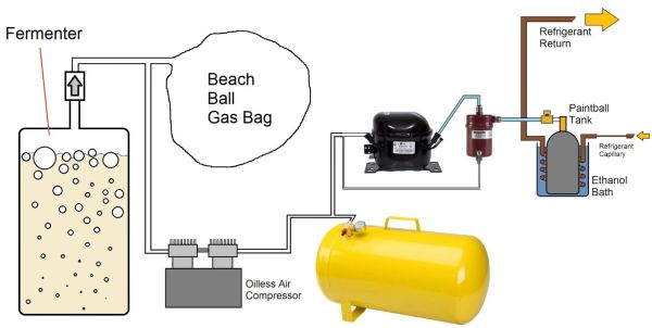
After previously using the fermenting of sugar to obtain ethanol fuel, [Hyperspace Pirate] figured that it’d be a waste to just blast the other half of the yeast production in the form of carbon dioxide into the air. This poses the slight problem that gaseous CO2 is fairly bulky, while compressing it into a liquid isn’t exactly for the faint of heart. This of course means that it’s a fun challenge, involving a beach ball, vapor-compression and various compressors.
Although at room temperature compressing CO2 into a liquid requires quite extreme pressures, if you lower it to freezing temperatures it becomes quite feasible to use more typical off-the-shell compressors.
In the video both oil-less and regular compressors are used, mostly because ultimately you want to get pure CO2 into the bottle, without oil or water. Here a few methods are explored, including a pre-cooler with the oil-less compressor as it cannot quite hit the same pressures. With a typical compressor linked to an oil-separator you can directly fill the tank, which is pretty nice, though even with this removal of water turned out to be a chore.
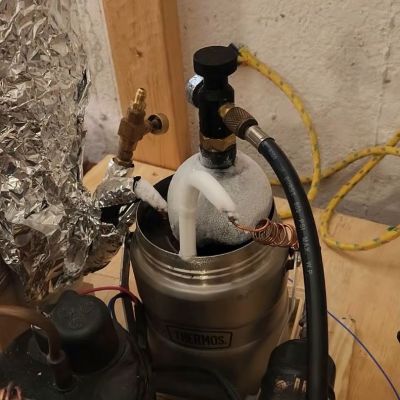
Desiccating the gas that comes out of the fermentation vat, is attempted using a converted water filter that’s filled with desiccant beads, but as the later tests show, this isn’t quite good enough to prevent moisture to make it into the bottle and clogging its nozzle. Of course, moisture here is more acceptable than oil for most applications, so with some more work this could be quite a feasible method to fill bottles with liquid CO2 for various nefarious applications like paintball guns and more.
The exciting part of buying a ‘broken, for parts’ off a site like EBay is that you rarely know exactly just how ‘broken’ it truly is. Even if the seller insists that it’s thoroughly buggered, you just might be able to eke out a fix with some out-of-the-box thinking and plucky ingenuity. Such was the case for [Dieter Vansteenwegen] who gambled on a cheap Canon 7D Mark II DSLR body that was sold for a mere €180 on account of said broken condition.
After confirming that the DSLR’s condition was basically as described by the seller, with nothing on the LCD or HDMI output and the auto-focus not working while partially pressing the trigger button, but still taking a picture when fully pressed. Sometimes it would also show a standard maintenance message on the LCD, so clearly it ought to be working. Maybe the camera’s processor was just being chronically unhappy about something, in which case an easy fix might be possible.
As anyone who has ever taken a digital camera apart knows, you do not simply pop them open for a quick look. Somewhere in the nightmarish contraption of flatflex cables, PCBs and endless sub-assemblies there might be a fault, but where to start? Fortunately with some support from the custom Canon firmware community Magic Lantern and the website Photo Parts UA for reference images he was able to start tracing a number of pertinent signals.
With the auto-focus hint as guide, this was traced back to the MPU, which turned out to have a floating signal on the auto-focus pin that got interpreted as ‘active’. Likely the internal pull-up got damaged due to the use of an external trigger module as there’s no real protection on these lines. One bodge wire later to create an external 3.3 V pull-up the DSLR happily sprung back to life.
In terms of parts this definitely was a cheap repair, but it comes with the prerequisite of having the skills and equipment to perform said repair. Still, massive props and congratulations to [Dieter] for saving this DSLR from being merely a device to be picked over for parts.
A lot has been made about the increase of automated traffic on the Internet, with the past years LLM-related crawlers having quite literally swarmed the picture here. Not only does this drive up traffic, it also increases load on web servers, whose owners find themselves faced with increased hosting costs. This recently led to The-Numbers.com going offline for a while as automated traffic was quite literally destroying their bottom line.
This saga is covered by [Stephen Follows], who had a chance to talk with the founder and CEO of the site, [Bruce Nash], after the site went basically offline for a few months. Since the website both licenses data for commercial purposes as well as offering the free access on its website, there were accusations of this being a ‘rug pull’.
The site was started in 1997, as a static HTML site on Geocities where [Bruce] provided box office analyses for investment purposes. Since that beginning traffic was generally polite, with human visitors and usually well-behaved search engine crawlers. Then around 2024 the first wave of scraper bots arrived, followed by a larger wave around December of 2025.
Despite implementing a few mitigations, such as LLM-targeted text, the increased traffic and the resulting load on a site architecture that was never designed for this ultimately led to a collapse. One of the major sources of traffic turned out to be from so-called ‘prediction markets’, like Polymarket, whose bots absolutely hammered the site.
Fortunately for [Bruce] and his team they do not rely on the free website for income, but they have had to massively rework the site’s architecture to bring back a semblance of the original features. As noted in the article, the amount of crawling traffic by these LLMs and ‘agentic AI’ tools is exponentially more than that for search engines, which makes this a major challenge.
Issues like these is why services such as Cloudflare are offering blocking features for such automated traffic. After all, unless such traffic is of use to you, you may as well treat it like a DDoS attack and cut it off at the root.
Seizure in zebrafish larva imaged using AO setup. (Credit: Bingxi Liu et al., Biomedical Optics Express, 2026)
Key to understanding something like epilepsy is to be able to record highly transient events in biological tissues. Generally this is done using light sheet microscopy, which provides effectively a 2D ‘slice’ of the tissue in question, but to observe a brief event in a larger biological system you need to be able to rapidly change the layer and focus between the virtual layers. This is what [Bingxi Liu] et al. al did using adaptive optics with an electrically tunable lens (ETL) in order to capture seizures in the brain of zebrafishes.
Their system can capture a volume of 499 × 499 × 150 μm3 at 4 volumes per second, which is large enough to fit optically transparent zebrafish larva into. The optical setup is shown in the above image, with the design based on the OpenSPIM platform for selective plane illumination microscopy.
Here the 488 nm laser provides the illumination (excitation) of the layer, while the 543 nm laser is for calibration purposes. The ETL is thus in the imaging path that allows for capturing by a digital camera, while a beam splitter directs part of the captured data to a Shack-Hartmann wave front sensor (SHWFS), which is part of the adaptive optics system.
After a seizure was induced in the zebrafish larva using the drug pentylenetetrazol the results were recorded using this system. It showed the seizure’s origin in the posterior brain, with subsequent propagation to the anterior before subsiding gradually over tens of seconds.
This system should be quite useful even outside of seizure research, as there are a lot of 3D systems in biology where having a relatively high-speed microscopic capture can be very revealing.
Community-led open source project hosting site Codeberg has formally announced that projects whose code is largely or fully machine-generated through LLMs and other ‘AI’ tools will no longer be welcome. This follows on the heels of a similar ban on cryptocurrency-related projects.
The community vote was on two issues, the first being the notion that scraping of project code for the use in LLMs should be forbidden, which was a motion that easily passed. The second motion was on disallowing projects whose code was substantially generated by LLMs like Claude, OpenAI Codex, and similar. This motion passed with 358 in favor versus 144 against.
In the earlier linked blog post the reasoning behind especially this second issue is expanded upon, covering not only ‘license whitewashing’, but also the direct and indirect hardware costs, with the expanding ‘AI’ datacenter hyperscaling having massively increased hardware costs for Codeberg over the past years, as the costs have been largely externalized.
Also covered is the aspect of these LLM-based tools destroying the OSS community, which is something that is backed up by recent studies. Even if we ignore that such LLM-tools are destroying the cognitive abilities of its users, there’s an argument to be made that if LLM-scraping is disallowed, then it’s consistent to also not allow LLM-generated code.
In the Terms of Use you can see these changes, both for LLMs and for cryptocurrency projects.
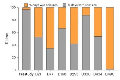
When an individual is born with genetic defects, there are a few ways to deal with the impact of the faulty genes. The most extreme solution is direct DNA editing to repair the mutation, while the treatment of symptoms with medication is the least invasive, though this comes with its own set of disadvantages. Antisense therapy keeps a middle ground here, by targeting the messenger RNA (mRNA) that forms the bridge between DNA and the translation into a functional protein by the ribosome.
In a recent study by [Olivia Kim-McManus] et al. antisense therapy with an allele-specific feature was demonstrated in two individuals with SCN2A mutations. These mutations had resulted in severe epilepsy and developmental disorders, due to how instrumental this gene is for normal functioning of the human central nervous system (CNS) where it regulates the initiation of action potentials.
Although SCN2A mutations are rarely inherited, for the approximately 1 in 80,000 affected the consequences can be quite dramatic. The two major types of mutations are classified as gain-of-function (GoF) and loss-of-function (LoF) with respectively hyper- and hyposensitivity of the resulting NAv1.2 sodium channels.
This translates especially in the case of GoF mutations into various symptoms, ranging from mild to severe (daily) epileptic attacks starting as an infant, stalled neurodevelopment and various types of autism (ASD). Often sodium channel blockers are prescribed for the GoF cases to limit epileptic attacks.
Usually with the responsible mutations only a single copy of the gene is affected, so while regular antisense therapy could be used, this would risk also modifying the healthy SCN2A mRNA copy. To get around this, an individualized treatment was developed, targeting the allele with the mutated gene for the two patients in the study: 9- and 14-year old boys with severe developmental and epileptic encephalopathies (DEE) that had left them with daily seizures and despite sodium-channel blockers and other typical medications.
Study outcome of the 14-year old boy with DEE after ASO therapy. (Credit: Kim-McManus et al., Nature Medicine, 2026)
During the trial, the 9-year old boy received 12 doses over 24 months of antisense oligonucleotides (ASOs) adapted to his affected allele, allowing for the cessation of the anti-seizure medication phenytoin, with an overall reduction in seizures. In the case of the 14-year old boy 8 doses were administered over 16 months, resulting in an average of two seizures a day being reduced to zero.
Although the focus of the study was on treating these seizures, by addressing the underlying cause of faulty mRNA transcriptions, changes in the neurodevelopmental state could also be observed. In particular language and motor skills improved, with erratic and irritable behavior reducing. The by then 15-year year old boy was able to walk unassisted, showing clear progression from the previous infantile state.
The advantage of ASOs over typical anti-seizure medication is of course that it directly addresses the faulty mRNA and thus the resulting faulty sodium channels. Since ASOs tend to hang around in a cell for a considerable amount of time, they could be quite a viable alternative treatment even for less severe cases. Whether early application of individualized ASOs in affected infants could lead to a more or less normal neurodevelopment would also be an interesting study question.
Naturally, directly addressing the faulty gene or upregulating the healthy gene would be the ideal and permanent solution, with research here also underway in mice models with the use of CRISPR-based tools.
Although it’s commonly suspected that migratory birds fly in a ‘V’ formation due to this saving energy for the birds in the slipstream, understanding the exact aerodynamics behind this and how it affects the way that the birds use their wings to maintain this optimal pattern. After all, unlike airplanes and cars, our feathered avian dinosaur friends need to flap their wings if they want to have any chance of staving off plummeting back to Earth. Recent research by Brown University researchers now have provided a simulated model that answers many questions.
The major question was how this would work in the up- and down-wash zones created in this type of formation, with every bird following the lead bird dealing with the vortices created by the flapping of the wings of the bird before them. These wake vortices are quite complex, and thus required careful modelling to make sense of them.
As described in the paper by [Olivia Pomerenk] et al., the model is based on northern bald ibises, taking into account live-bird measurements for validation of the model. The main effect that can be observed is a reduced flapping amplitude, leading to an 11% energy savings for the birds in the leader’s wake.
The main advantage of having such a model is of course that it provides insight into the kinematic and aerodynamic mechanisms, meaning the ability to model virtual flocks of birds, predict the efficiency of specific in-flight configurations, and apply the lessons to swarms of drones, or whatever else we want to put in the air.
 After previously using the fermenting of sugar to obtain ethanol fuel, [Hyperspace Pirate] figured that it’d be a waste to just blast the other half of the yeast production in the form of carbon dioxide into the air. This poses the slight problem that gaseous CO2 is fairly bulky, while compressing it into a liquid isn’t exactly for the faint of heart. This of course means that it’s a fun challenge, involving a beach ball, vapor-compression and various compressors.
 After confirming that the DSLR’s condition was basically as described by the seller, with nothing on the LCD or HDMI output and the auto-focus not working while partially pressing the trigger button, but still taking a picture when fully pressed. Sometimes it would also show a standard maintenance message on the LCD, so clearly it ought to be working. Maybe the camera’s processor was just being chronically unhappy about something, in which case an easy fix might be possible.