Creating A PCB In Everything: Introduction

engineering-drawingA few years ago, I wrote a few columns titled Making A Thing. These columns were a tutorial of sorts for several different 3D modeling programs. This column wasn’t meant to be a complete guide to modeling an object in OpenSCAD or SolidWorks, it was just step-by-step instructions on how to make one specific thing with one specific piece of software.

More than a few people in the Hackaday community found this column useful or at the very least an interesting pedagogical device. When starting out with any kind of productivity software, you don’t need to know how to do everything, you just need to know how to do the most common tasks.

Since the Making A Thing column was so popular, I felt it was time to revive this idea with another design task we often face. As you have already guessed, we’re going to be making printed circuit boards. Continuing the unique tutorial format created in the previous iteration of this column, Making a PCB will build one specific circuit in multiple EDA suites.

The Circuit

The entire concept of demonstrating how to build one thing in a specific software package necessitates a model thing. Before I even begin writing the first Making A PCB column, I need to design something that’s sufficiently complex but still relatively simple, and something that’s hopefully somewhat useful. Breakout boards are extremely simple, perhaps too much. In the course of these programs, I’ll need to demonstrate how to make a part in each specific software suite, so fewer pins are better.

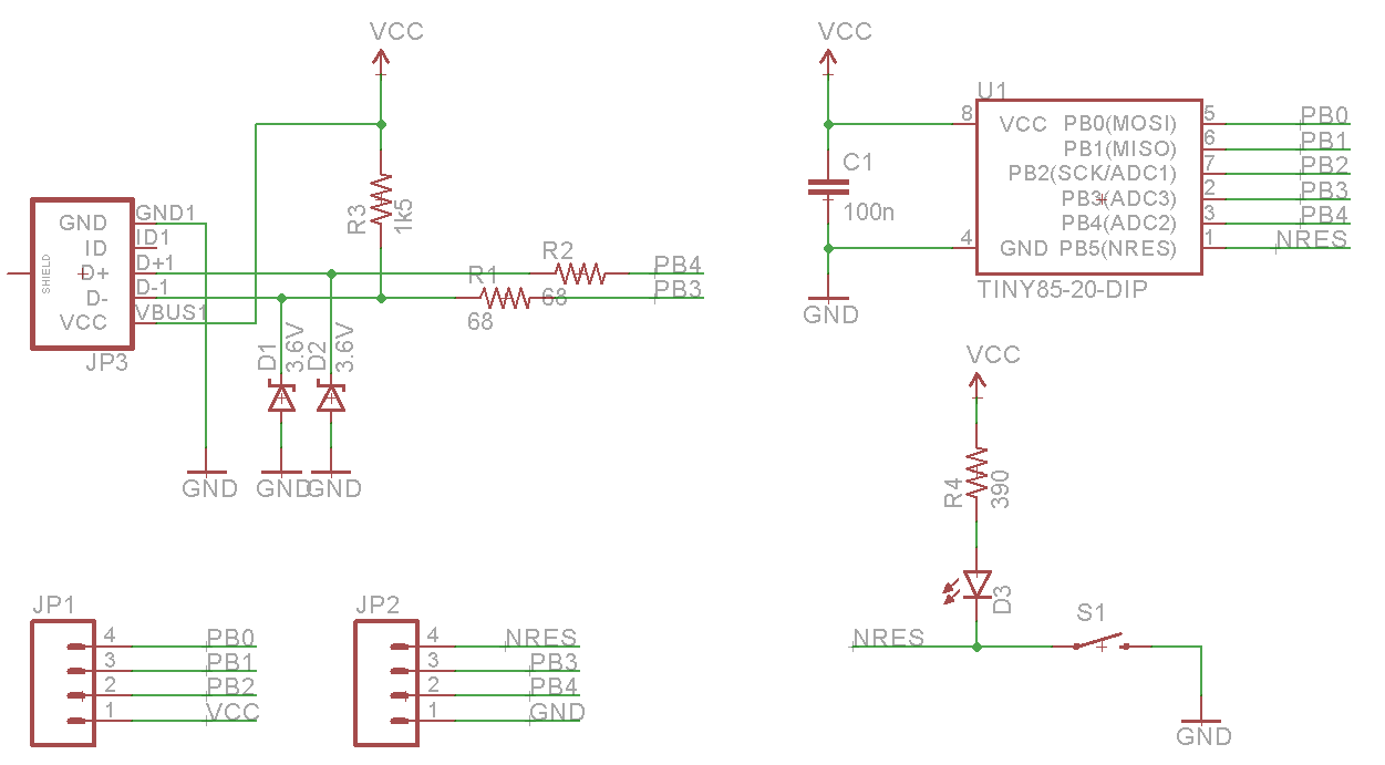
Lacking any creativity of my own, I’ve settled on a very small ATtiny85 Arduino derivative from Tim a.k.a. [cpldcpu]. Tim’s Nanite 85 is an exceptionally small Arduino-compatible board based on the ATtiny85, complete with a USB port, LED, and a few pins of I/O. It’s simple but sufficiently complex to give an introduction to a PCB design suite.

I’m not going to outright copy Tim’s Nanite 85, though. It’s much clearer if parts aren’t stacked on top of each other, and I’d like to give myself a little breathing room on the layout. I’ve redesigned the circuit of the Nanite 85 to use mostly through-hole parts on a slightly larger board. I’m calling my version the Nanite Wesley, and if you get that reference, thumbs up for you.

ThingPCBSch
The schematic for the Nanite Wesley
naniteboard
The Nanite Wesley board. Copper pours not shown

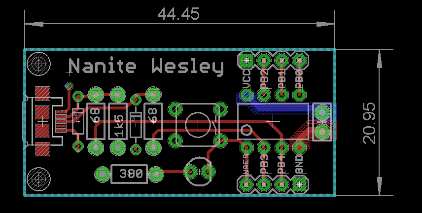
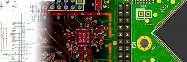
Is this how a board should be laid out? No, absolutely not. I could probably do this as a single-layer board. This is a very inefficient layout, and I like rounded corners on my boards. It’s good enough, though, and it works. This is meant to be a tutorial on how to use a PCB design package, not a tutorial on how to design a PCB. Your criticisms in this regard are noted and ignored.

What These Tutorials Will Consist Of

You cannot use a PCB design package until you know how to make a part. Yes, Eagle has wonderful libraries for almost everything you can imagine, KiCad has plenty of parts on the Internet, and if you’re using a cloud-based PCB software, almost everything will be provided for you. If you make a PCB, eventually you’ll have to make your own part, though, and each tutorial will begin with making a DIP-8 ATtiny85. Everything else on this board is a jellybean part. Either way, the process of making a part and package for a Zener is the same as making one for a microcontroller.

The next part of the tutorial will consist of schematic capture. This means placing the parts in the schematic, drawing wires between the pins and pads, and naming them. From there, it’s time to actually make a board, and this means dropping the parts down, putting traces between all the pins, doing the board outline, pouring copper, and mechanical considerations.

With the schematic and board designed, it will be time to send it off to a fab house. For Eagle and KiCad, this is easy; OSHpark accepts Eagle .brd and KiCad .pcb files, but this is cheating. We’re going to use CAM to generate real Gerber files. If you make enough PCBs, you’ll have to learn it eventually.

Caveats and Poor Design

There are a lot of things that go into making a ‘proper’ PCB, including isolation, direct traces to decoupling capacitors, making sure pixies don’t go around sharp corners and a thousand other items that won’t be discussed in these tutorials. There’s a reason I won’t be discussing this. This is a guide on how to use a PCB design tool, not how to design a PCB.

What else should I do?

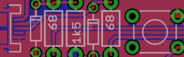
As you can probably guess from the schematic above, the first PCB software I’m going to cover is Eagle. KiCad is on the list, as is Fritzing, Altium CircuitMaker, and OrCAD. In the interests of putting PCB design in a historical context, I have a copy of AutoTRAX and an old DOS machine. I’ll also be covering a few of the cloud-only design tools such as Upverter.

That’s enough software suites to get started, but as with the Making A Thing series, I’m going to be looking for suggestions from the peanut gallery. I can’t change the circuit I’m making, as that’s the entire point of this series, but I am looking for suggestions on other tools to cover. What else can I do? Want me to grab a piece of copper clad board, sticker overlays, and some photostatic film? I can do that. Are you at a web-based EDA startup, and want some free advertising? Leave a note in the comments.

Thanks to our efforts to slowly improve the backend of Hackaday, you’ll be able to access all the Making A PCB In Everything posts from the series list below.

The Future Of Eagle CAD

Last week, Autodesk announced their purchase of CadSoft Eagle, one of the most popular software packages for electronic design automation and PCB layout.

Eagle has been around for nearly thirty years, and has evolved to become the standard PCB design package for electronic hobbyists, students, and engineering firms lead by someone who learned PCB design with Eagle. The reason for this is simple: it’s good enough for most simple designs, and there is a free version of Eagle. The only comparable Open Source alternative is KiCad, which doesn’t have nearly as many dedicated followers as Eagle.  Eagle, for better or worse, is a standard, and Open Source companies from  Sparkfun to Adafruit use it religiously and have created high-quality libraries of parts and multiple tutorials

I had the chance to talk with [Matt Berggren], former Hackaday overlord who is currently serving as the Director of Autodesk Circuits. He is the person ultimately responsible for all of Autodesk’s electronic design products, from Tinkercad, 123D, Ecad.io, and project Wire, the engine behind Voxel8, Autodesk’s 3D printer that also prints electronics. [Matt] is now the master of Eagle, and ultimately will decide what will change, what stays the same, and the development path for Eagle.

Continue reading “The Future Of Eagle CAD”

Reinventing VHDL Badly

A few years ago, Philip Peter started a little pet project. He wanted to build his own processor. This really isn’t out of the ordinary – every few months you’ll find someone with a new project to build a CPU out of relays, logic chips, or bare transistors. Philip is a software developer, though, and while the techniques and theory of building hardware haven’t changed much in decades, software development has made leaps and bounds in just the past few years. He’s on a quest to build a CPU out of discrete components.

Search the Internet for some tips and tricks for schematic capture programs like KiCad and Eagle, and you’ll find some terrible design choices. If you want more than one copy of a very specific circuit on your board, you have to copy and paste. Circuit simulation is completely separate from schematic capture and PCB design, and unit testing – making sure the circuit you designed does what it’s supposed to do – is a completely foreign concept. Schematic capture and EDA suites are decades behind the curve compared to even the most minimal software IDE. That’s where Philip comes in. By his own admission, he reinvented VHDL badly, but he does have a few ideas that are worth listening to.

Continue reading “Reinventing VHDL Badly”

KiCad Traducido Al Español

KiCad ya es una gran herramienta para la captura esquemática y el diseño de PCB, pero el software sólo funciona si es posible utilizarlo. Para los mil millones de personas que no hablan inglés, esto significa que el idioma es la barrera más grande al momento de utilizar el mejor software para desarrollo de hardware. En los últimos meses, [ElektroQuark] ha estado liderando esfuerzos de localización al español de KiCad y estos se encuentran finalmente completados. También ha iniciado un foro de KiCad en idioma español para llevar el desarrollo de software hacia uno de los idiomas más hablado del planeta.

SpanishMientras que ha habido otros intentos por localizar KiCad a otros idiomas, la mayoría de estos proyectos se encuentran incompletos. En una actualización de KiCad hace algunos meses, la localización al español ya contaba con algunas cadenas ya traducidas, pero no demasiadas. Los esfuerzos de [ElektroQuark] han acercado KiCad a millones de hablantes nativos de español, no solo algunos de sus menús.

El español es la segunda lengua más hablada del planeta, mientras que el inglés es la tercera. Teniendo en cuenta solamente este hecho, parece absurdo que casi todas las herramientas de software para capturas esquemáticas y diseño de PCB sean localizados sólo al chino o al inglés. Los esfuerzos de [ElektroQuark] por localizar KiCad al español son un gran avance para un ya impresionante software.

Eagle To KiCad Made Easy

One barrier for those wanting to switch over from Eagle to KiCad has been the lack of a way to convert existing projects from one to the other. An Eagle to KiCad ULP exists, but it only converts the schematic, albeit with errors and hence not too helpful. And for quite some time, KiCad has been able to open Eagle .brd layout files. But without a netlist to read and check for errors, that’s not too useful either.

[Lachlan] has written a comprehensive set of Eagle to KiCad ULP scripts to convert schematics, symbols and footprints. Board conversion is still done using KiCad’s built in converter, since it works quite well, and we were able to successfully convert two projects from Eagle. The entire process took only about 10 to 15 minutes of clean up after running the scripts.

The five scripts and one include file run sequentially once the first one is run. [Lachlan]’s scripts will convert Eagle multi sheet .sch to KiCad multi sheets, place global and local net labels for multi sheets, convert multi part symbols, build KiCad footprint modules and symbol libraries from Eagle libraries, create a project directory to store all the converted files, and perform basic error checking. The Eagle 6.xx PCB files can be directly imported to KiCad. The scripts also convert Via’s to Pads, which helps with KiCad’s flood fill, when Via’s have no connections — this part requires some manual intervention and post processing.

KiCad Utilities Generate Parts; Track Costs

The popularity of KiCad keeps increasing, and not only are more people converting to it and using it for their projects, but there’s also a growing number of folks actively contributing to the project in the form of libraries, scripts and utilities to improve the work flow.

KiPart

[Dave Vandenbout] a.k.a [xesscorp] has written a couple of utilities for KiCad. When working with large multi pin parts such as micro-controllers, creating a schematic symbol from scratch using the traditional KiCad schematic library editor can be quite tedious. KiPart is a python script that uses a CSV table as its input to generate the KiCad schematic symbol and is able to create multi-part symbols too. Usage is quite simple. The csv file needs a part name on its first row. The next row contains the headers. ‘Pin’ number and Pin ‘Name’ are the minimum required. Additionally, you can add in ‘Unit’, ‘Side’, ‘Type’, and ‘Style’. Unit is used when defining multi-unit parts. Side decides the location of the pin, Type its function, and Style is its graphic representation. Running the KiPart python script then results in a nice KiCad schematic symbol. Besides, KiPart can specifically generate schematic symbols for the Xilinx 7-Series FPGAs and the Cypress PSoC5LP. There are a whole host of options to customize the final output, for example ordering pin placement based on pin number, or pin name or pin function. Source files can be obtained from the [xesscorp] Github repository.

KiCost

KiCost
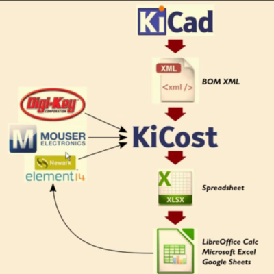
Another useful utility from [xesscorp] is KiCost. It is intended to be run as a script for generating part-cost spreadsheets for circuit boards developed with KiCad. The one piece of information you need to add to your schematic parts is a manufacturers part number. The KiCost Python script then processes the BOM XML file, reading the manufacturer part number, scraping the web sites of several popular distributors for price and inventory data, and creating a costing spreadsheet. You can grab the source files from the KiCost Github repository.

Check the two videos below where [Dave] walks through the two utilities.

Thanks to [RoGeorge] for sending in this tip by commenting on the Open Source FPGA Pi Hat built by [Dave] that we featured recently.

Continue reading “KiCad Utilities Generate Parts; Track Costs”

KiCad 4.0 Is Released

If you’re a KiCad user, as many of us here at Hackaday are, you’ll be elated to hear that KiCad 4.0 has just been released! If you’re not yet a KiCad user, or if you’ve given it a shot in the past, now’s probably a good time to give it a try. (Or maybe wait until the inevitable 4.0.1 bugfix version comes out.)

If you’ve been using the old “stable” version of KiCad (from May 2013!), you’ve got a lot of catching-up to do.

The official part footprint libraries changed their format sometime in 2014, and are all now hosted on GitHub in separate “.pretty” folders for modularity and ease of updating. Unfortunately, this means that you’ll need to be a little careful with your projects until you’ve switched all the parts over. The blow is softened by a “component rescue helper” but you’re still going to need to be careful if you’re still using old schematics with the new version.

The most interesting change, from a basic PCB-layout perspective, is the push-and-shove router. We’re looking for a new demo video online, but this one from earlier this year will have to do for now. We’ve been using various “unstable” builds of KiCad for the last two years just because of this feature, so it’s awesome to see it out in an actual release. The push-and-shove router still has some quirks, and doesn’t have all the functionality of the original routers, though, so we often find ourselves switching back and forth. But when you need the push-and-shove feature, it’s awesome.

If you’re doing a board where timing is critical, KiCad 4.0 has a bunch of differential trace and trace-length tuning options that are something far beyond the last release. The 3D board rendering has also greatly improved.

Indeed, there are so many improvements that have been made over the last two and a half years, that everybody we know has been using the nightly development builds of KiCad instead of the old stable version. If you’ve been doing the same, version 4.0 may not have all that much new for you. But if you’re new to KiCad, now’s a great time to jump in.

We’ve covered KiCad hacks before, and have another article on KiCad add-on utilities in the pipeline as we write this. For beginners, [Chris Gammell]’s tutorial video series is still relevant, and is a must-watch.

Thanks [LC] for the newsworthy tip!