Active Ideal Full Bridge Rectifier Using TEA2208T

Everyone loves a full-wave bridge rectifier, but there’s no denying that they aren’t 100% efficient due to the diode voltage drop. Which isn’t to say that with some effort we cannot create an ideal bridge rectifier using active components, as demonstrated by [Mousa] with an active bridge circuit. This uses the NXP TEA2208T active bridge rectifier controller, along with the requisite four MOSFETs.

Comparing a diode bridge rectifier with an active bridge rectifier. (Credit: Mousa, YouTube)

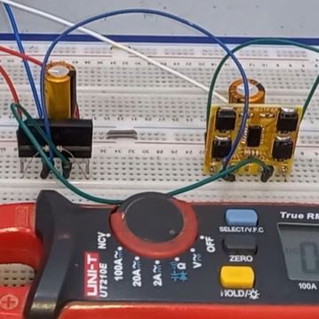
Taking the circuit from the datasheet, a PCB was created featuring four FDD8N50NZ MOSFETs in addition to the controller IC. These were then compared to a diode-based bridge rectifier, showing the imperfections with the latter when analyzing the output using an oscilloscope.

As expected, the active rectifier’s output was also one volt higher than the diode bridge rectifier, which is another small boost to overall efficiency. According to NXP’s product page, there’s about a 1.4% efficiency gain at 90 VAC, with the chip being promoted for high-efficiency operations. When you consider that many designs like computer PSUs feature one or more diode bridge rectifiers often strapped to heatsinks, the appeal becomes apparent. As for [Mousa], he put this particular board in his laboratory PSU instead of the diode bridge rectifier, because why not.

Perhaps the biggest impediment to using an active rectifier is the cost, with the TEA2208T coming in at $4 on DigiKey for a quantity of 100, in addition to the MOSFETs, PCB, etc. If power efficiency isn’t the goal, then some wasted power and an aluminium heatsink is definitely cheaper.

Continue reading “Active Ideal Full Bridge Rectifier Using TEA2208T”

Vacuum Sputtering With A Homemade Magnetron

“You can never be too rich or too thin,” the saying goes, and when it comes to coatings, it’s true that thinner is often better. The way to truly thin coatings, ones that are sometimes only a few atoms thick, is physical vapor deposition, or PVD, a technique where a substance is transformed into a vapor and condensed onto a substrate, sometimes using a magnetron to create a plasma.

It sounds complicated, but with a few reasonable tools and a healthy respect for high voltages, a DIY magnetron for plasma sputtering can get you started. To be fair, [Justin Atkin] worked on his setup for years, hampered initially by having to settle for found parts and general scrap for his builds. As with many things, access to a lathe and the skills to use it proved to be enabling, allowing him to make custom parts like the feedthrough for the vacuum chamber as well as a liquid-cooled base, which prevents heat from ruining the magnets that concentrate the plasma onto the target metal. Using a high-voltage DC supply made from old microwave parts, [Justin] has been able to sputter copper films onto glass slides, with limited success using other metals. He also accidentally created a couple of dichroic mirrors by sputtering with copper oxides rather than pure copper. The video below has some beautiful shots of the ghostly green and purple glow.

A rig such as this opens up a lot of possibilities, from optics to DIY semiconductors. It may not be quite as elaborate as some PVD setups we’ve seen, but we’re still pretty impressed.

Continue reading “Vacuum Sputtering With A Homemade Magnetron”