Sputtering Daguerreotypes, Batman!

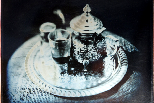
The Daguerreotype was among the earliest photographic processes, long before glass plates or film, that relied on sensitizing a thin layer of silver on top of a copper plate. The earliest Daguerreotype plates were made physically, by rolling a copper-silver plate thinner and thinner until the silver layer was just right. Good luck finding a source of Daguerreotype plates made this way in 2022. (There are electroplating methods, but they all end up with chemically contaminated silver.)

On the other hand, magnetron sputtering is a process of depositing pure metal in thin layers using plasma, high voltages, and serious magnets, and [Koji Tokura] is making his own sputtered Daguerreotype plates this way, giving him the best of both worlds: the surreal almost-holographic quality of the Daguerreotype with the most difficult film preparation procedure imaginable.

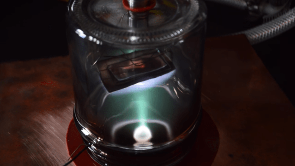
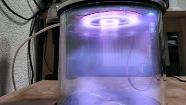
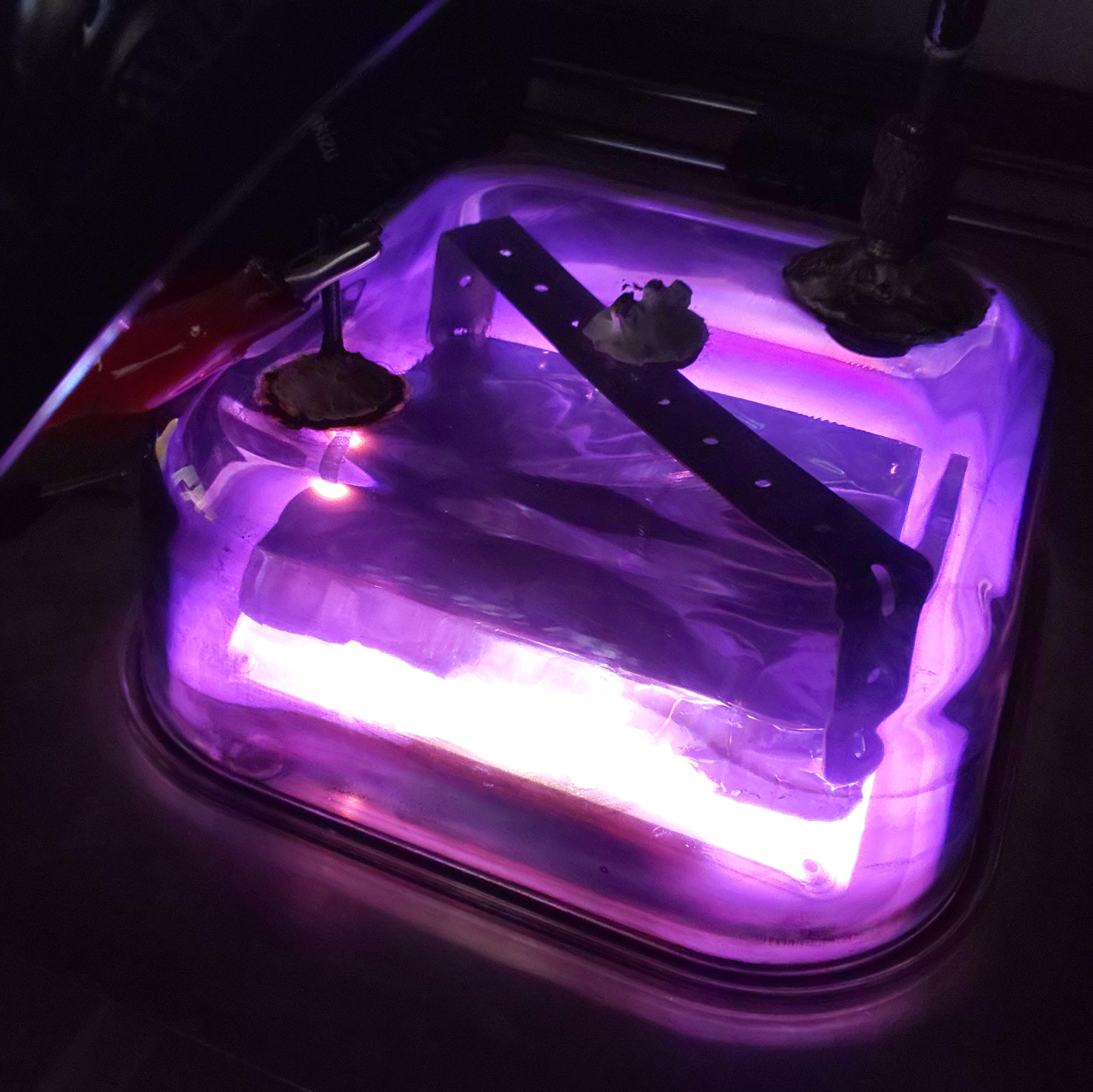
The star of the show is [Koji]’s sputtering rig, which consists of a Tupperware glass sandwich box as a vacuum chamber and a microwave oven transformer as the high voltage source. In use, he pumps the chamber down, introduces a small amount of argon, and then lights up the plasma. The high voltage accelerates the plasma ions into a sheet of silver, and the silver particles that get knocked free coat the copper plate. A strong magnet creates a local plasma, which accelerates the coating procedure, but since [Koji] only had a relatively small magnet, he scans the plate with the magnet, using a scavenged 2D pen plotter mechanism.

Check out his video on the Hackaday.io page, and his Daguerreotype gallery as well. (We don’t think that they were all made with this procedure.)

The result is a chemically pure Daguerreotype plate produced in a seriously modern way, and we’d love to see the images in person. In these days of disposable images made by the AIs in your cell phone, it’s nice to see some people taking photography in strange directions. For instance, maybe you’d like to make your own ultra-large collodion plates. Or something else? If you do, show us!

[Ben Krasnow] Rolls Old School Camera Out For Photolithography

In a time when cameras have been reduced to microchips, it’s ironic that the old view camera, with its bellows and black cloth draped over the viewscreen for focusing, endures as an icon for photography. Such technology appears dated and with no application in the modern world, but as [Ben Krasnow] shows us, an old view camera is just the thing when you want to make homemade microchips. (Video, embedded below.)

Granted, the photolithography process [Ben] demonstrates in the video below is quite a bit upstream from the creation of chips. But mastering the process on a larger scale is a step on the way. The idea is to create a high-resolution photograph of a pattern — [Ben] chose both a test pattern and, in a nod to the season, an IRS tax form — that can be used as a mask. The camera he chose is a 4×5 view camera, the kind with lens and film connected by adjustable bellows. He found that modifications were needed to keep the film fixed at the focal plane, so he added a vacuum port to the film pack to suck the film flat. Developing film has always been magical, and watching the latent images appear on the film under the red light of the darkroom really brings us back — we can practically smell the vinegary stop solution.

[Ben] also steps through the rest of the photolithography process — spin coating glass slides with photoresist, making a contact print of the negative under UV light, developing the print, and sputtering it with titanium. It’s a fascinating process, and the fact that [Ben] mentions both garage chip-maker [Sam Zeloof] and [Justin Atkin] from the Thought Emporium means that three of our favorite YouTube mad scientists are collaborating. The possibilities are endless.

Continue reading “[Ben Krasnow] Rolls Old School Camera Out For Photolithography”

Titanium Coating Is Actually Pretty Straightforward

[Justin] enjoys tinkering in his home lab, working on a wide variety of experiments. Recently, he’d found much success in coating objects with thin layers of various metals with the help of a DC sputtering magnetron. However, titanium simply wouldn’t work with this setup. Instead, [Justin] found another way.

As it turns out, coating with titanium is quite achievable for even the garage operative. Simply run current through a titanium wire, heating it above 900 degrees in a vacuum. This will create a shower of titanium atoms that will coat virtually anything else in the chamber. [Justin] was able to achieve this with little more than some parts from Home Depot, a vacuum pump, and a cheap glass jar. He was able to produce a nice titanium oxide finish on a knife blade, giving that classic rainbow look. Coating crystals was less straightforward, but the jet black finish achieved was impressive nonetheless.

[Justin] plans to upgrade his vacuum rig further, and with better process control, we’d expect even better results. The earlier work is also very relevant if you’re interested in creating fine coatings of other materials. Video after the break. Continue reading “Titanium Coating Is Actually Pretty Straightforward”

Vacuum Sputtering With A Homemade Magnetron

“You can never be too rich or too thin,” the saying goes, and when it comes to coatings, it’s true that thinner is often better. The way to truly thin coatings, ones that are sometimes only a few atoms thick, is physical vapor deposition, or PVD, a technique where a substance is transformed into a vapor and condensed onto a substrate, sometimes using a magnetron to create a plasma.

It sounds complicated, but with a few reasonable tools and a healthy respect for high voltages, a DIY magnetron for plasma sputtering can get you started. To be fair, [Justin Atkin] worked on his setup for years, hampered initially by having to settle for found parts and general scrap for his builds. As with many things, access to a lathe and the skills to use it proved to be enabling, allowing him to make custom parts like the feedthrough for the vacuum chamber as well as a liquid-cooled base, which prevents heat from ruining the magnets that concentrate the plasma onto the target metal. Using a high-voltage DC supply made from old microwave parts, [Justin] has been able to sputter copper films onto glass slides, with limited success using other metals. He also accidentally created a couple of dichroic mirrors by sputtering with copper oxides rather than pure copper. The video below has some beautiful shots of the ghostly green and purple glow.

A rig such as this opens up a lot of possibilities, from optics to DIY semiconductors. It may not be quite as elaborate as some PVD setups we’ve seen, but we’re still pretty impressed.

Continue reading “Vacuum Sputtering With A Homemade Magnetron”

Practical Plasma For Thin-Film Deposition

[Nixie] wants to sputter. We know, who doesn’t? But [Nixie] has a specific purpose for his sputtering: thin-film deposition, presumably in support of awesome science. But getting to that point requires a set of tools that aren’t exactly off-the-shelf items, so he’s building out a DIY sputtering rig on the cheap.

If you’re not familiar with sputtering, that’s understandable. In this context, sputtering is a process that transfers particles from one solid to another by bombarding the first solid with some sort of energetic particles, usually electrons or a plasma. When properly controlled, sputtering has applications from mass spectrometry to the semiconductor industry, where it’s used to either deposit thin films on silicon wafers or etch them away selectively.

No matter the application, sputtering needs a stable stream of plasma. [Nixie] has posted a series of articles on his blog walking us through his plasma experiments, from pulling a really strong vacuum to building a high-voltage power supply from a microwave oven transformer. It’s a project that needs a deep well of skills and tools, like glassworking, machining, and high-voltage electronics. Check out the plasma in the video below.

Will [Nixie] be using this for a DIY fab lab? Will it be used to make homebrew LEDs? The world waits to hear.

Continue reading “Practical Plasma For Thin-Film Deposition”

Scanning Electron Microscope Adds To Already Impressive Garage Lab

When you’re a high schooler who built a semiconductor fab in your garage, what’s next on your agenda? Why, adding a scanning electron microscope to your lab, naturally. How silly of you to ask.

When last we stumbled across the goings on in the most interesting garage in New Jersey, [Sam Zeloof] was giving a tour of his DIY semiconductor fabrication lab and showing off some of the devices he’s made there, including diodes and MOSFETs. As impressive as those components are, it’s the equipment he’s accumulated that really takes our breath away. So adding an eBay SEM to the mix only seems a natural progression, and a good reason to use some of the high vacuum gear he has. The video below shows [Sam] giving a tour of the 1990s-vintage instrument and shows images of various copper-sputtered samples, including a tick, which is apparently the state bird of New Jersey.

SEM hacks are by no means common around here, but they’re not unheard of. [Ben Krasnow] has used his to image cutting tools and phonograph records in action, and there are a few homebrew SEMs kicking around too. But our hats are off to [Sam] for yet another acquisition and a great tutorial to boot.

Continue reading “Scanning Electron Microscope Adds To Already Impressive Garage Lab”