Liquid Metal Ion Thrusters Aren’t Easy

What do scanning electron microscopes and satellites have in common? On the face of things, not much, but after seeing [Zachary Tong]’s latest video on liquid metal ion thrusters, we see that they seem to have a lot more in common than we’d initially thought.

As you’d expect with such a project, there were a lot of false starts and dead ends. [Zach] started with a porous-emitter array design, which uses a sintered glass plate with an array of tiny cones machined into it. The cones are coated in a liquid metal — [Zach] used Galinstan, an alloy of gallium, indium, and tin — and an high voltage is applied between the liquid metal and an extraction electrode. Ideally, the intense electric field causes the metal to ionize at the ultra-sharp tips of the cones and fling off toward the extraction electrode and into the vacuum beyond, generating thrust.

Getting that working was very difficult, enough so that [Zach] gave up and switched to a slot thruster design. This was easier to machine, but alas, no easier to make work. The main problem was taming the high-voltage end of things, which seemed to find more ways to produce unwanted arcs than the desired thrust. This prompted a switch to a capillary emitter design, which uses a fine glass capillary tube to contain the liquid metal. This showed far more promise and allowed [Zach] to infer a thrust by measuring the tiny current created by the ejected ions. At 11.8 μN, it’s not much, but it’s something, and that’s the thing with ion thrusters — over time, they’re very efficient.

To be sure, [Zach]’s efforts here didn’t result in a practical ion thruster, but that wasn’t the point. We suspect the idea here was to explore the real-world applications for his interests in topics like electron beam lithography and microfabrication, and in that, we think he did a bang-up job with this project.

Continue reading “Liquid Metal Ion Thrusters Aren’t Easy”

Silicone Devices: DIY Stretchable Circuits

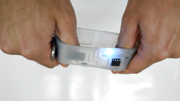
Flexible circuits built on polyimide film are now commonplace, you can prototype with them at multiple factories, at a cost that is almost acceptable to your average hacker. Polyimide film is pretty tough for something so thin, but eventually it will tear, and with larger components, bend radii are quite restricted. But what about stretchable circuits, as in circuits you can flex, twist and stretch? Let us introduce silicone devices. A research group from Hasselt University, Belgium, have been prototyping making truly flexible, silicone-based circuit substrates, managing to integrate a wide range of SMT component types with a dual layer interconnect, with vias and external contacts.

It should be possible to reproduce the process using nothing more special than your average Makerspace CO2 laser cutter, and a couple of special tools that can be easily made — a guide for that is promised — it is purely a matter of gathering a few special materials, and using off-cuts you have lying around for the rest. The interconnect uses Galinstan, which is a low melting point alloy of gallium, indium, and tin. Unfortunately, this material is fairly expensive and cannot be shipped by air due to the gallium content, without specialised handling, at considerable expense. But that aside, other than some acrylic sheets, some vinyl, copper foil and a few sprays, nothing is beyond reach.

The construction process is reverse to what we normally see, with the components and copper contact plates placed first, on to a primed vinyl sheet. This sheet is laser marked with the component outlines to enable them to be corrected placed. Yes, that’s right, they’re using a laser cutter to mark vinyl, a chlorine-containing plastic. Hold on to that thought for a bit.

Insulating layers and substrate layers are constructed by blade-coating with a layer of clear silicone. Interconnect layers are formed by sticking a fresh vinyl sheet onto the exposed contacts and laser cutting just though it to expose the pads and the interconnect traces. Next the fancy Galinstan is applied by brush and the vinyl stencil removed. Rinse and repeat for the next layer of insulating silicone, more circuit traces, then use the laser cutter to precisely etch through the via regions to allow more metalisation to be added. Finally a coating of silicone is applied over the whole assembly, the laser is again used to etch the silicone away from the contact pads, and with a little solder tinning of these, you’re done. Simple, if only our Makerspaces didn’t have rules against laser cutting vinyl.

This was clearly a very brief overview, here is a very detailed instructables guide ready for you, as well as a formal research paper, detailing why this came about and why you might want to try this yourself.

If you’re into custom wearables, you might remember this earlier piece about silicone circuits, and this one weird organic-looking thing from the same time-frame.

Continue reading “Silicone Devices: DIY Stretchable Circuits”