Synthesis Of Goldene: Single-Atom Layer Gold With Interesting Properties

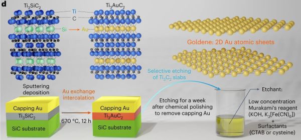
The synthesis of single-atom layer versions of a range of atoms is currently all the hype, with graphene probably the most well-known example of this. These monolayers are found to have a range of mechanical (e.g. hardness), electrical (conduction) and thermal properties that are very different from the other forms of these materials. The major difficulty in creating monolayers is finding a way that works reliably and which can scale. Now researchers have found a way to make monolayers of gold – called goldene – which allows for the synthesis of relatively large sheets of this two-dimensional structure.

In the research paper by [Shun Kashiwaya] and colleagues (with accompanying press release) as published in Nature Synthesis, the synthesis method is described. Unlike graphene synthesis, this does not involve Scotch tape and a stack of graphite, but rather the wet-etching of Ti3Cu2 away from Ti3AuC2, after initially substituting the Si in Ti3SiC2 with Au. At the end of this exfoliation procedure the monolayer Au is left, which electron microscope studies showed to be stable and intact. With goldene now relatively easy to produce in any well-equipped laboratory, its uses can be explored. As a rare metal monolayer, the same wet exfoliation method used for goldene synthesis might work for other metals as well.

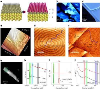
Molybdenene whiskers. (Credit: Sahu et al., 2023)

Introducing Molybdenene As Graphene’s New Dirac Matter Companion

Amidst all the (well-deserved) hype around graphene, it’s important to remember that its properties are not unique to carbon. More atoms can be coaxed into stable 2-dimensional configuration, with molybdenene previously theoretically possible. This is now demonstrated by Tumesh Kumar Sahu and colleagues in a recent Nature Nanotechnology article, through the manufacturing of a 2D molybdenum-based material which they showed to be indeed molybdenene. Essentially, this is a 2D lattice of molybdenum atoms, a configuration in which it qualifies as Dirac matter, just like graphene. For those of us unfamiliar with Dirac materials, this gentle introduction by Jérôme Cayssol in Comptes Rendus Physique might be of use.

Manufacturing process of molybdenene. (Credit: Sahu et al., 2023)

In order to create molybdenene, the researchers started with molybdenum disulfide (MoS2), which using a microwave-assisted field underwent electrochemical transformation into whiskers that when examined turned out to consist out of monolayers of Mo. The sulfur atoms were separated using a graphene sheet. As is typical, molybdenene sheets were exfoliated using Scotch tape, in a process reminiscent of the early days of graphene research.

Much like graphene and other Dirac materials, molybdenene has many potential uses as a catalyst, as cantilever in scanning electron microscope (SEM) tips, and more. If the past decades of research into graphene has demonstrated anything, it is that what once seemed more of a novelty, suddenly turned out to have endless potential in fields nobody had considered previously. One of these being as coatings for hard disk platters, for example, which has become feasible due to increasingly more efficient ways to produce graphene in large quantities.

$1 Graphene Sensor Identifies Safe Water

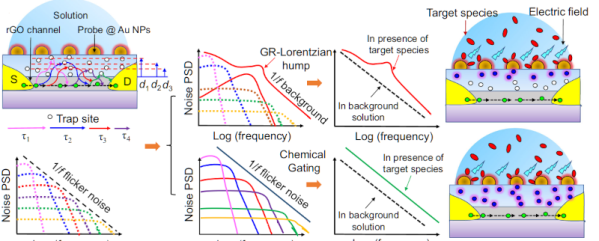
If you live in a place where you can buy Arduinos and Raspberry Pis locally, you probably don’t spend much time worrying about your water supply. But in some parts of the world, it is nothing to take for granted, bad water accounts for as many as 500,000 deaths worldwide every year. Scientists have reported a graphene sensor they say costs a buck and can detect dangerous bacteria and heavy metals in drinking water.

The sensor uses a GFET — a graphene-based field effect transistor to detect lead, mercury, and E. coli bacteria. Interestingly, the FETs transfer characteristic changes based on what is is exposed to. We were, frankly, a bit surprised that this is repeatable enough to give you useful data. But apparently, it is especially when you use a neural network to interpret the results.

What’s more, there is the possibility the device could find other contaminants like pesticides. While the materials in the sensor might have cost a dollar, it sounds like you’d need a big equipment budget to reproduce these. There are silicon wafers, spin coating, oxygen plasma, and lithography. Not something you’ll whip up in the garage this weekend.

Still, it is interesting to see a FET used this way and a cheap way to monitor water quality would be welcome. Using machine learning with water sensors isn’t a new idea. Of course, the sensor is one part of the equation. Monitoring is the other.

Easy Graphene Production With A Laser Engraver

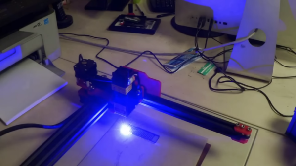
Graphene isn’t easy to produce at scale. But making small batches of graphene is doable in a few ways. [Robert Murray-Smith] decided to try producing “flash graphene.” This requires a big capacitor bank that is moderately expensive, so he decided to explain a different technique he read about using an ordinary laser cutter. Check it out in the video below.

We were a little disappointed that he didn’t actually make any graphene this time. He has, however, used other methods in other videos to create some type of graphene. In fact, he has many similar videos going back quite a ways as well as applications with concrete, capacitors, and more. We understand that this method doesn’t produce monolayer graphene, but actually creates a graphene “foam” with interesting properties. [Robert] talks about recent papers that show you can grow graphene on things other than Kapton tape using this method.

Continue reading “Easy Graphene Production With A Laser Engraver”

Noninvasive Sensors For Brain–Machine Interfaces Based On Micropatterned Epitaxial Graphene

As fun as brain-computer interfaces (BCI) are, for the best results they tend to come with the major asterisk of requiring the cutting and lifting of a section of the skull in order to implant a Utah array or similar electrode system. A non-invasive alternative consists out of electrodes which are placed on the skin, yet at a reduced resolution. These electrodes are the subject of a recent experiment by [Shaikh Nayeem Faisal] and colleagues in ACS Applied NanoMaterials employing graphene-coated electrodes in an attempt to optimize their performance.

Impedance values of eight-channel FEG and eight-channel HPEG sensor systems placed on the occipital area of the head. (Faisal et al., 2023)

Although external electrodes can be acceptable for basic tasks, such as registering a response to a specific (visual) impulse or for EEG recordings, they can be impractical in general use. Much of this is due to the disadvantages of the ‘wet’ and ‘dry’ varieties, which as the name suggests involve an electrically conductive gel with the former.

This gel ensures solid contact and a resistance of no more than 5 – 30 kΩ at 50 Hz, whereas dry sensors perform rather poorly at >200 kΩ at 50 Hz with worse signal-to-noise characteristics, even before adding in issues such as using the sensor on a hairy scalp, as tends to be the case for most human subjects.

In this study, they created electrode arrays in a number of configurations, each of which used graphene as the interface material. The goal was to get a signal even through human hair — such as on the back of the head near the visual cortex — that would be on-par with wet electrodes. The researchers got very promising results with hex-patterned epitaxial graphene (HEPG) sensors, and even in this early prototype stage, the technique could offer an alternative where wet electrodes are not an option.

While the subject is complex, brain-computer interfaces don’t have to be the sole domain of research laboratories. We recently covered an open hardware Raspberry Pi add-on that can let you experiment with detecting and filtering biosignals from the comfort of your own home.

The Challenges Of Producing Graphene In Quantity

We’ve all heard the incredible claims made about graphene and its many promising applications, but so far the wonder-material has been held back by the difficulty of producing it in large quantities. Although small-scale production was demonstrated many years ago using basic Scotch tape, producing grams or even kilograms of it in a scalable industrial process seemed like a pipedream — until recently. As [Tech Ingredients] demonstrates in a new video, the technique of flash Joule heating of carbon may enable industrial graphene production.

The production of this flash graphene (FG) was first demonstrated by Duy X. Luong and colleagues in a 2020 paper in Nature, which describes a fairly straightforward process. In the [Tech Ingredients] demonstration it becomes obvious how easy graphene manufacturing is using this method, requiring nothing more than carbon black as ingredient, along with a capacitor bank, vacuum chamber and a number of reasonably affordable items.

Perhaps best of all is that no refinement or other complicated processes are required to separate the produced graphene from the left-over carbon black and other non-graphene products. Using multiple of these carbon black-filled tubes in parallel, producing graphene could conceivably be scaled up to industrial levels. This would make producing a few kilograms of graphene significantly easier than coating hard drive platters with the substance.

Continue reading “The Challenges Of Producing Graphene In Quantity”

A Transistor? Memory? Wait, It’s Both!

What do you get if you cross graphene, hexagonal boron nitride, and tungsten diselenide? Well, according to researchers at Hunan University, you get a field effect transistor that can act as both a switching element or a memory cell. The partial floating-gate field-effect transistor or PFGFET uses 2D van der Waals heterostructures to deal with isolated atomic layers. The paper in Nature is unfortunately behind a pay wall, but you can read a summary over on [TechExplore].

The graphene acts as the gate, and the transistor can be switched between n-type behavior and p-type behavior. It can also be configured as a switching element or as a memory element similar to an EEPROM cell.

One advantage of having configurable transistor types is that a single transistor structure can produce CMOS or complementary circuits. Traditionally, a CMOS IC has two different transistor structures and often producing one of them requires extra effort.

The configuration takes place by applying a control voltage pulse. A negative control voltage produces a p-type FET and a positive voltage configures the same transistor as an n-type. If you don’t have access to the paper, the figures available online offer a good bit of insight into the device’s design.

If you want to learn more about ordinary MOSFETs, we talk about them often. You can also get the skinny on CMOS from [Bil Herd].