mobo_salvage

PCB Parts Salvaging Made Easy

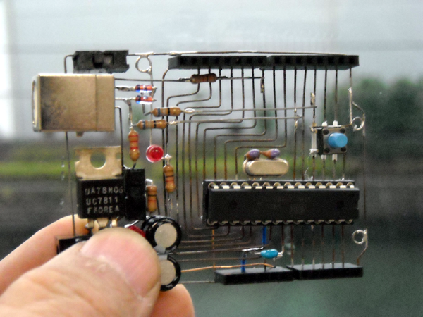
Take a moment to think about how many old or damaged computer motherboards you have tossed away over the years. Sure we try to repurpose everything we can, but reclaiming electronic components from complex devices can be overly time consuming if you don’t have the proper means of doing so.

Ideally, if we were to try removing components from a motherboard, an old stove or an unused toaster oven would be great. If you didn’t have either item at your disposal, you could always attack the board with a soldering iron and some braid – but who has the time for that?

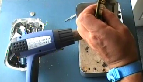
[Giorgos Lazaridis] over at PCBHeaven put together a quick video demonstrating his favorite technique for salvaging components after a motherboard has outlived its usefulness. Using a 2000W heat gun, a few hand tools, and couple of metal pans, he had the entire board stripped bare in about 30 minutes time. He talks about some of the best parts he has discovered while salvaging and points out a few hard-to-find items that can be easily obtained by tearing down a motherboard.

Sure his process might not be as easy as inverting a PCB in an oven, but his method is cheap, portable, and takes up very little space.

Keep reading to see [Giorgos’] video demonstration and don’t forget to check out some of the other cool stuff he has done in the past, such as his temperature-controlled soldering station, this acrylic bender, or this bench top function generator.

Continue reading “PCB Parts Salvaging Made Easy”

PCBs Without Any Substrate

[Kimio Kosaka] is taking the concept of free-formed circuits to the next level with O’Baka Project No.7. It’s a fully functioning Arduino board, without the board. The traces are there and provide all of the support for the rest of the hardware. You can imagine the fragility of the package so it won’t be a surprise to learn that O’Baka Project means ‘stupid’ project.

We don’t think this manufacturing process is completely worthless. The ‘board’ seen above looks quite interesting and might be a good idea when building a show-piece where you want the circuitry to be seen. [Kimio] describes the process he used to achieve this look. The first step is to design a single-sided circuit board; he used EagleCAD. After printing out the traces he used 0.46mm steel wire to trace out each connection. Now heat up that soldering iron – [Kimio] recommends using high-acid flux to ease the process of soldering to the steel.

We think this would nicely compliment projects like LED cubes that use the circuit itself as a support structure. See this Arduino alternative from several different angles in the video after the break.

Continue reading “PCBs Without Any Substrate”

Hackaday Links: March 27, 2011

Magnified glasses

A late hacking session, and parts-on-hand came together as the inspiration for [BadWolf’s] magnified glasses with LED lighting.

Pendulum Printer

This orb, when swung like a pendulum, prints images by dropping ink out the bottom. A processing sketch works in conjuction with a Wii Remote and an IR LED in the orb to sense when the print head is in just the right position for dispensing ink.

ITead PCB fab house tips and tricks

[Flemming] uses a PCB fab house called ITead Studio. We hadn’t heard of it before but if you consider giving it a try make sure you look over his tips and tricks about the service before submitting your designs.

Katamari Bookmarklet

[Spi] wrote in to let us know about this Java Bookmarklet he came across that lets you turn any webpage into a Katamari Damacy level. It’s a pretty clever bit of code.

Color-picker pen

Here’s a pen concept inspired by Photoshop. On one end there’s a scanner that lets you pick your color from any physical object. Then just turn it around and write with the exact same color. Now go out and make this reality! [Thanks Frank]

Test Your Etching Chops With PCB Map Making

pcb_map

[Martin] had been using standard perf board for most of his electronics projects, but as he was starting to utilize more surface mount ICs, he quickly realized that it was time to start making his own PCBs. Having never etched any PCBs using the toner transfer method, he figured it was as good a time as any to give it a try.

Rather than make a board for a particular project, he decided to try his hand at etching a very detailed map of the Paris Metro as a test pattern instead. He grabbed a large image of the subway map, then printed it out on the back of a supermarket flyer. He attached it to his PCB and ran it through a lamination machine to transfer the toner. He figured that the laminator would be easier than an iron to use, and was right for the most part. The only issue he had was that the laminator did not generate enough heat, so he supplemented the its heat output with a hair dryer.

When everything was said and done, he had a pretty good looking PCB on his hands. Most of the Metro tracks and text came out just fine, though he admits there is a bit of room for improvement. It looks nice when mounted in a frame, though we would love to see a functional circuit made out of a PCB map like that. Heck, we’d even settle for a double-sided PCB with a street-level map on one side an the Metro on the other!

Direct To PCB Resist Printing Requires Minimal Additional Components

epson_inkjet

Printing PCBs using the toner transfer method works pretty well, but there are some downsides, such as incomplete trace transfers and the like. HackHut user [rucalgary] decided to go the inkjet route instead, and picked up an Epson printer on clearance at his local electronics shop. This method is not new by any means, but his printer conversion is one of the simplest we’ve seen as it does not rely on any additional sensors to function.

Once he got home, he tore the printer down immediately, removing the paper input and output trays as well as the scanner bed. After all of the extraneous parts were removed, he got to work raising up the printer head, as well as the printer head rest mechanism. He mentions that the latter component is absolutely crucial to proper functionality down the line. Once the print head and its associated components were relocated, he added a pair of aluminum rails for feeding his print tray into the machine.

With everything complete, he filled up a spare cartridge with ink (he says that MISPRO yellow works best) and ran some test boards through. He is quite pleased with how things turned out, and is more than happy to give you a quick tour of his completed printer via the video below.

Continue reading “Direct To PCB Resist Printing Requires Minimal Additional Components”

Give KiCAD A Try. Here’s How

Up to this point we’ve used Eagle CAD as our exclusive PCB design and schematic layout tool. But [Brian] has inspired us to try something different thanks to his KiCAD tutorial.

KiCAD is an open source printed circuit board design tool. Since we like to rock the Linux here at Hackaday getting our hands on this was as easy as:

 sudo apt-get install kicad

The version in the Ubuntu 10.04 repositories is a bit older but seemed to work just fine. [Brian] jumps right in with one of our most dreaded tasks on Eagle, designing your own parts. He knows of a nice online tool for automatic KiCAD part generation and walks through the process of building a voltage regulator and importing it for use in your own personal library From there it’s off to layout a power supply schematic for a breadboard PSU. The lesson continues with board layer, as well as the process used for exporting data for PCB fab house. We think this tutorial works well if you’re already familiar with PCB layout using a different software package but it moves a bit fast if this is your first time.

KiCAD seems like a nice tool and we’ve heard from many advocates in the comments over the years. Look for our next PCB design to be on KiCAD as we just need to use it for a while before passing judgement.

Simple PCB Etchant Made From Chemicals You Can Put In Your Mouth

etching_test

[Stephen] often finds the need to make his own PCBs at home, and when he got the urge to do some etching recently, he realized that he was fresh out of “Ferret Chloride and Bureaucratic Acid*.” Undeterred by his empty chemical cabinet, he poked around in his kitchen mixing together anything and everything that might have the ability to strip copper from a PCB.

Now, we don’t necessarily recommend this course of action, but it seems that he finally hit upon a winner. He discovered a formula that can be made at home from simple and safe household ingredients which does the job quite nicely. A fair warning however, standard ferric chloride disposal procedures need to be followed when using this solution.

If you want to know what he concocted in his kitchen as well as the chemistry behind it, you will have to visit his site, we won’t ruin it for you. You can however, see the solution at work in the video we have posted below.

*His joke, not ours

Continue reading “Simple PCB Etchant Made From Chemicals You Can Put In Your Mouth”