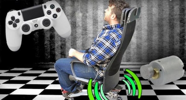
A PS-3 controller has an unbalanced motor inside that vibrates your hand whenever you crash a car into a wall or drive it off a cliff and hit the rocks below but [Rulof Maker] wanted that same feeling all over his body. So he added a serious unbalanced motor to his favorite gaming chair to make his whole body vibrate instead.
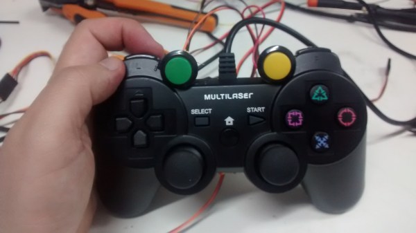
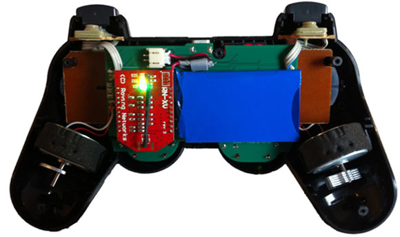
To do that he opened up the controller and found the wires going to the unbalanced motor. There he added a small relay, to be activated whenever the motor was energized. Wires from that relay go to a female connector mounted in the side of the controller, keeping the controller small and lightweight.
Next he needed to attach a much bigger unbalanced motor to the underside of his favorite gaming chair. For the unbalanced mass he poured concrete powder and molten lead into a tin can mold and attached the result to the motor’s shaft. Using a piece of wood he attached the motor to the chair’s underside.
All that was left was to power the motor and turn it on when needed. For that he wired up a bigger relay, with the relay’s coil wired to a male connector to plug into the PS-3 controller. Now when the PS-3 wants to vibrate, that relay is energized. All that was left was to wire the relay’s normally open switch, the motor and a power cord in series, plug it into the wall socket, and he was ready to shake.
Continue reading “Gaming Chair Gives Full Body Feeling To Collisions”