Learning Verilog For FPGAs: Hardware At Last!

Getting into FPGA design isn’t a monolithic experience. You have to figure out a toolchain, learn how to think in hardware during the design, and translate that into working Verliog. The end goal is getting your work onto an actual piece of hardware, and that’s what this post is all about.

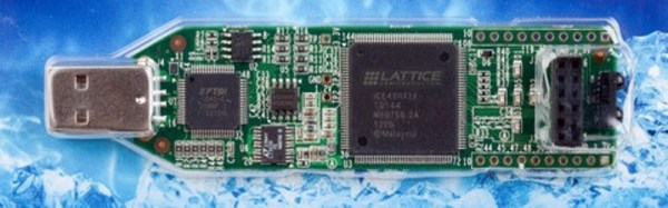
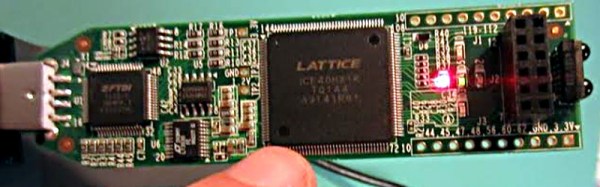
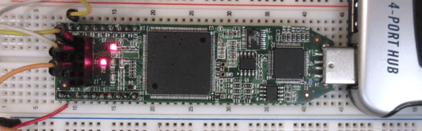
In the previous pair of installments in this series, you built a simple Verilog demonstration consisting of an adder and a few flip flop-based circuits. The simulations work, so now it is time to put the design into a real FPGA and see if it works in the real world. The FPGA board we’ll use is the Lattice iCEstick, an inexpensive ($22) board that fits into a USB socket.

Like most vendors, Lattice lets you download free tools that will work with the iCEstick. I had planned to use them. I didn’t. If you don’t want to hear me rant about the tools, feel free to skip down to the next heading.

Continue reading “Learning Verilog For FPGAs: Hardware At Last!”

Learning Verilog For FPGAs: Flip Flops

Last time I talked about how to create an adder in Verilog with an eye to putting it into a Lattice iCEstick board. The adder is a combinatorial circuit and didn’t use a clock. This time, we’ll finish the demo design and add two clocked elements: a latch that remembers if the adder has ever generated a carry and also some counters to divide the 12 MHz clock down to a half-second pulse to blink some of the onboard LEDs.

Why Clocks?

Clocks are an important part of practical digital design. Suppose you have a two input AND gate. Then imagine both inputs go from zero to one, which should take the output from zero to one, also. On paper, that seems reasonable, but in real life, the two signals might not arrive at the same time. So there’s some small period of time where the output is “wrong.” For a single gate, this probably isn’t a big deal since the delay is probably minuscule. But the errors will add up and in a more complex circuit it would be easy to get glitches while the inputs to combinatorial gates change with different delays.

Continue reading “Learning Verilog For FPGAs: Flip Flops”

Learning Verilog For FPGAs: The Tools And Building An Adder

Over the last year we’ve had several posts about the Lattice Semiconductor iCEstick which is shown below. The board looks like an overgrown USB stick with no case, but it is really an FPGA development board. The specs are modest and there is a limited amount of I/O, but the price (about $22, depending on where you shop) is right. I’ve wanted to do a Verilog walk through video series for awhile, and decided this would be the right target platform. You can experiment with a real FPGA without breaking the bank.

In reality, you can learn a lot about FPGAs without ever using real hardware. As you’ll see, a lot of FPGA development occurs with simulated FPGAs that run on your PC. But if you are like me, blinking a virtual LED just isn’t as exciting as making a real one glow. However, for the first two examples I cover you don’t need any hardware beyond your computer. If you want to get ready, you can order an iCEstick and maybe it’ll arrive before Part III of this series if published.

Continue reading “Learning Verilog For FPGAs: The Tools And Building An Adder”