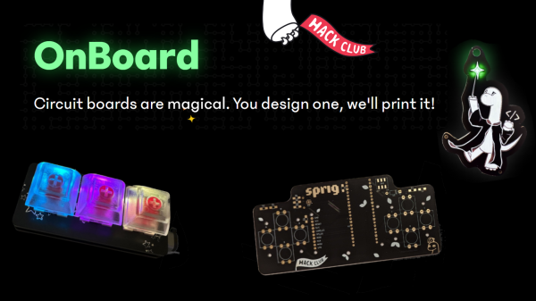
[Hack Club] is a nonprofit network of coder and maker clubs for teenage high school students around the world. With an impressive reach boasting clubs in about 400 schools, they serve approximately 10,000 students. Their OnBoard program asserts, “Circuit boards are magical. You design one, we’ll print it!”
Any teenage high school student can apply for a [Hack Club] OnBoard Grant to have their Printed Circuit Board design fabricated into real hardware. The process starts by designing a PCB using any tool that can generate Gerber files. The student then publishes their design on GitHub and submits the Gerber files to a PCB manufacturer.
A screenshot from the board house showing the completed design upload and production cost is the main requirement of the grant application. If approved, the grant provides up to $100 to cover PCB manufacturing costs.
OnBoard encourages collaboration, community, and friends. Designers can share their projects and progress with [Hack Club] teens around the world. Those who are working on, or have completed, their own circuit board designs can share support and encouragement with their peers.
Example hardware projects from [Hack Club] include Sprig, an open-source handheld game console based on the Raspberry Pi Pico microcontroller. Teen makers can explore the example OnBoard projects and then it’s… three, two, one, go!
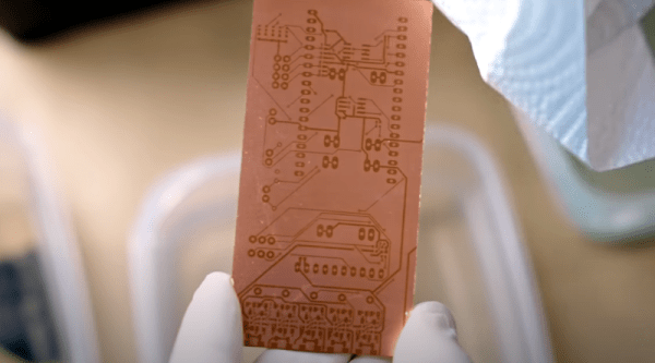
We always enjoy [Thomas Sanladerer’s] 3D printing videos. But his latest isn’t only about 3D printing. He shows how he uses a DLP printer — which has UV light, after all — to expose PC board blanks with great results. Honestly, once we heard the idea, we immediately saw how that could work it is surprising more people aren’t taking advantage of their DLP printers like that. Of course, [Thomas] does his usual thorough treatment of the topic.
Really, this isn’t exactly 3D printing even though it uses a 3D printer. Exposing boards with UV light and artwork is an old process that has been around for years, usually using transparency film and a UV light source. With a printer, you can create artwork digitally and the UV light source is already there.
You hold in your hand a circuit board from a product you didn’t make. How does the thing work? What a daunting question, but it’s both solvable and approachable if you know what you’re doing. The good news is that Eric Schlaepfer knows exactly what he’s doing and boiled down the process of reverse engineering printed circuit boards into this excellent workshop. It was presented live during the 2020 Hackaday Remoticon, and the edited video, which you’ll find below, was just published. Slides for the talk have been published on the workshop project page.
Printed circuit boards are a fundamental part of both of commercial electronic equipment and of the projects we feature here on Hackaday. Many of us have made our own, whether done so from first principles with a tank of etchant, or sent off as a set of Gerbers to a PCB fab house.
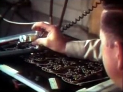
To say that the subject of today’s Retrotechtacular is the manufacture of printed circuit boards might seem odd, because there is nothing archaic about a PCB, they’re very much still with us. But the film below the break is a fascinating look at the process from two angles, both for what it tells us about how they are still manufactured, and how they were manufactured in 1969 when it was made.
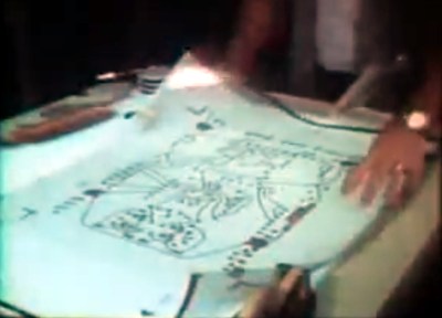
Board artwork laid out at four-times actual size
Tektronix were as famous for the manufacturer of particularly high quality oscilloscopes back then as they are now. The Tektronix ‘scopes of the late 1960s featured several printed circuit boards carrying solid-state electronics, and were manufactured to an extremely high standard. The film follows the manufacturing process from initial PCB layout to assembled board, with plenty of detail of all production processes.
In 2017 you would start a PCB design in a CAD package, but in 1969 the was incredibly manual. Everything was transcribed by hand from a paper schematic to transparent film. Paper mock-ups of component footprints four times larger than actual size are placed on a grid, and conductors drawn in pencil on an overlaid piece of tracing paper. Then the pads and pattern of tracks are laid out using black transfers and tape on sheets of film over the tracing paper, one each for top and bottom of the board. A photographic process reduces them to production size onto film, from which they can be exposed and etched in the same way that you would in 2017.
Pantograph drilling machine uses a manually moved styuls on a template to drill six boards at once
Most of the physical process of creating a PCB has not changed significantly since 1969. We are shown the through-plating and gold plating processes in detail, then the etching and silkscreening processes, before seeing component installation and finally wave soldering.
What are anachronistic though are some of the machines, and the parts now robotised that were done in 1969 by hand. The PCB drilling is done by hand with a pantograph drill for small runs, but for large ones a fascinating numerically-controlled drilling rig is used, controlled by punched tape without a computer in sight. Component placement is all by hand, and the commentator remarks that it may one day be done by machine.
The film remains simultaneously an interesting look at PCB production and a fascinating snapshot of 1960s manufacturing. It’s probable that many of the Tek ‘scopes made on that line are still with us, they’re certainly familiar to look at from our experience at radio rallies.
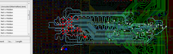
[Helentronica] has been using Altium Designer to lay out PC boards since he was a student. Now as a freelancer, he felt like he didn’t quite know all that he wanted to know. Keep in mind he’d done multilayer boards with BGAs and LVDS routing, so he was no neophyte. He decided to spend about $200 on an advanced course from Fedevel Academy. In this day where everything is free on the Internet, is it worth paying $200 to watch some videos?
[Helentronica] probably weighed the same question. However, he was interested in the course project which is an open-source computer module with an i.MX6 processor, 1 GB of DDR3 SDRAM and lots of expansion options. In fact, the ad copy that sold him was:
You will be practicing on a real high-speed board with 1.2GHz CPU and DDR3, PCIE, SATA, HDMI, LVDS, 1Gb Ethernet and more
He completed the course. Was it worth it? We won’t spoil the story, but you should check out his post and find out. Even if you don’t want to drop $200 or you don’t use Altium, you will probably pick up some tips on PC board layout.