Join [Matt Martin], ASIC designer at Keysight, for this week’s Hack Chat.
Every week, we find a few interesting people making the things that make the things that make all the things, sit them down in front of a computer, and get them to spill the beans on how modern manufacturing and technology actually happens. This is the Hack Chat, and it’s happening this Friday, March 17, at noon PDT (20:00 UTC).
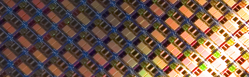
 [Matt] has been working at Agilent / Keysight since 2007 as an ASIC designer. The work starts with code that is synthesized into logic gates. After that, [Matt] takes those gates and puts them into silicon. He’s worked with processes from 0.13um to 28nm. Turning code into silicon is still a dark art around here, and if you’ve ever wanted to know how all of this works, this is your chance to find out.
Here’s How To Take Part:
 Our Hack Chats are live community events on the Hackaday.io Hack Chat group messaging.
Log into Hackaday.io, visit that page, and look for the ‘Join this Project’ Button. Once you’re part of the project, the button will change to ‘Team Messaging’, which takes you directly to the Hack Chat.
You don’t have to wait until Friday; join whenever you want and you can see what the community is talking about.
Upcoming Hack Chats
We’ve got a lot on the table when it comes to our Hack Chats. On March 24th, we’re going to argue the merits of tube amplifiers in audio applications. In April, we have [Samy Kamkar], hacker extraordinaire, to talk reverse engineering.
Because I’ve never had the opportunity to do so, and because these Hack Chat announcement posts never get many comments anyway, I’m going to throw this one out there. What would it take to build out a silicon fabrication plant based on technology from 1972? I’m talking about a 10-micrometer process here, something that might be able to clone a 6502. Technology is on our side — a laser printer is cheaper than a few square feet of rubylith — and quartz tube heaters and wire bonding machines can be found on the surplus market. Is it possible to build a silicon fab in your garage without going broke? Leave your thoughts in the comments, and then bring them with you to the Hack Chat this Friday.


How much is Agilent paying HaD for this ad campaign?
Nothing.
When will you grow up?
Because Keysight, an international Corp they creates test equipment for companies who build and test the electrics you, and the rest of the world own. I’m sure they are they need the income from the 5 hackers on Hacksaw who can afford $10k for a scope.
How dare HackADay mention the credentials of a real engineer giving us all quality content FOR FREE.
Damn Mike, quit being such a shill!
On the note of stupid demands, what’s with two of the three HaD meetings being in Cali – oddly enough there are other places where engineers like, like Portland or Seattle!
How hard is it to design an FPGA?
Probably not very… the internals of an ice40hx fpga are pretty standard fair. Although the best you are going to fab in your garage with tens of thousands of dollars of equipment is probably more like a CPLD than an FPGA…
http://ic.ese.upenn.edu/pdf/pdluts_fpt2013.pdf
that should give you a good idea of the complexity.. about 150 transistors per 4-LUT so… 150,000 transistors needed to build something similar to ice40 1k + transistors for ram (lets be generous and say 32k transistors) so somewhere around 200,000k+ transistors to build a simple FPGA. By Contrast a MOS 6502 only has 3,510 transistors…
You can take some shortcuts and knock probably about %25 off your transistor count… (multi valued vs binary luts) but it is still much more than a simple processor.
I am NOT an expert on FPGA design. However, I can take a guess….
The LUTs themselves are not hard — pretty much any 1st year graduate could come up with the logic to do that. However, the LUTs are NOT the hard part. Let me explain….
1) There are a LOT more things in an FPGA than just the configurable logic. DDR interface, multipliers, SERDES, clock generators, Ethernet interfaces, embedded processors, and the entire IO system. Not to mention the fabric to program everything up. Several of these will require analog designers in addition to the usual digital design staff.
2) Testing can be rough. When designing custom silicon, one of the first rules to make testing possible is to completely avoid internal tri-state busses. Period. I won’t go into the details, but if you want to emulate a processor bus with a dozen different devices on the data bus, you don’t use tri-states, you use a giant 12-input mux. Well, as near as I can tell, tri-state bus drivers are used for the long-distance interconnects. Testing these using the usual methods is tough.
3) I would imagine that the silicon is the easy part. You have to make the entire software tool chain that will allow you to actually USE this wonderful chip. I would not be surprised at all if the Xilinx software team is larger than the hardware team.
The big problem would probably be the chemicals, getting them, using them and handling the waste. Even for a 10µm process things have to be clean and pure to avoid hard to track problems. For a hobby project the lithography isn’t too hard, some have used modified microscopes (e.g. https://gmwgroup.harvard.edu/pubs/pdf/757.pdf ) and using a scanning laser wouldn’t be too expensive (break down a DVD or blu ray writer).
Assuming you’d be using something like a demijohn sized vacuum chamber with a small wafer like 4″ you’d need quite tiny amounts of chemicals, and could probably drain them all off in a small waterbottle and drop them in McDonalds garbage…. don’t get caught doing that…. okay fine, don’t actually do that.
They’re not allllll that nasty, half of them they sell at hardware stores to pour down the drain in quantities 1000 times greater (sodium hydroxide etc.) Some become nasty and EPA fodder in industrial quantities, but yah, teaspoons here.
Have done similar things in a university undergraduate lab that’s run quite a bit better with more funding than a university lab. You definitely need a very good mask aligner (i.e. very good microscope setup), at least a few furnaces for the different dopants, etc. Even then, it’s very difficult to even get one transistor working, let alone hundreds at ten micron (the yield is quite low on most sections). It turns out it’s very difficult to get a meaningful number of transistors at a time in an /integrated/ circuit, without being extremely clean, extremely meticulous, using properly graded reagents, and not skimping on /all/ of the little steps you need (using the right etchants to have the right selectivity, etc.)
Basically, even after you get the equipment working, it’s going to be a hell of a lot of practice to get good enough to align things to even sort of work.
that’s run quite a bit better and with more funding than a typical hobbyist lab*
Also, protip for anyone going down the lithographic route, from extensive testing on PCB resists on many printer models: most toners and inkjets are not actually opaque enough for good photolithography. I recall you were pretty much equally likely to fail whether it was an inkjet or laser printer (in my sample set, anyway), and printing settings did not intuitively improve the situation. A nice trick, if your inkjet has good enough page-to-page feed alignment, is to print twice on the same transparency – this is opaque enough in almost all cases, though results in very poor vertical alignment in almost all printers.
So an everyday “laser printer” is not going to cut it, most of the time. Additionally, I’ve found using third party vs non-third party toner makes a big difference. The only toner I found that consistently worked to the specifications required by PCB resists was from a very high end Xerox printer at a public library. I recommend purchasing a step wedge to debug the issue. If you ever tried doing photolithography based on what some guy posted online, and failed miserably, even perhaps with a similar brand of printer, this is probably why.
Anywho, you’re probably going to need a much better mask than just a laser print in most cases if you want to try to do photolithography on silicon. Plus, the dot size on most laser printers is too big for a reliable 10 micron process.
A sick “D” sign?