Through-hole assembly means bending leads on components and putting the leads through holes in the circuit board, then soldering them in place, and trimming the wires. That took up too much space and assembly time and labor, so the next step was surface mount, in which components are placed on top of the circuit board and then solder paste melts and solders the parts together. This made assembly much faster and cheaper and smaller.
Now we have embedded components, where in order to save even more, the components are embedded inside the circuit board itself. While this is not yet a technology that is available (or probably even desirable) for the Hackaday community, reading about it made my “holy cow!” hairs tingle, so here’s more on a new technology that has recently reached an availability level that more and more companies are finding acceptable, and a bit on some usable design techniques for saving space and components.
Copper Components
First, let’s talk about components that are made out of the copper itself, because this is accessible and widely used. With the right math and layout, it’s possible to create resistors, capacitors, fuses, and antennas out of copper. This kind of stuff is done all the time.
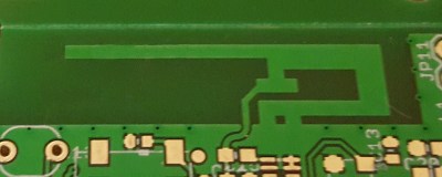
The heated build platform of your 3D printer is likely just an FR4 PCB with a single spiral trace. Because the copper has some resistance, and that resistance is a function of the current and width of the trace, some careful calculation will give you a board that heats up to the right temperature without damaging the board.
You can do impedance matching with traces, or make them wind around in a single skinny line to make a single low value resistor (keeping in mind that tolerance is terrible because of copper thickness variance). Or you can place two traces right next to each other to create a small capacitor. This costs you board space, but saves you from having to place a component. You can also create a fuse by pinching a current-carrying trace in a single point so that with enough current it heats up and blows the trace. Granted, you can’t replace this fuse, but it could be considered a last line of defense to protect the rest of the electronics if all else fails.
There are also trace antennas, found inside nearly every small RF gadget. The Inverted F antenna is particularly suited for 2.4 GHz radios, and saves a lot of money and physical space.
Embedded Components
What’s really exciting is that components are now being embedded inside circuit boards. There are lots of reasons and advantages:
- Saves physical space, both vertically and on the PCB plane
- Easier routing and shorter traces
- Less parasitic capacitance
- Better EMI shielding (an oscillator or crystal can be between layers, surrounded on top and bottom by copper pours)
- Heat management
- Reliability
- Difficult to reverse engineer
There’s cost and additional process, though, and requires a lot of coordination with the PCB fabricators and assembly houses. The greatest reason to do this is size reduction, so unless you are building a “world’s smallest” or doing large volume runs of smartphones, this is not something you will want to do.
Chip ON board is old news; we’ve seen the blobs of black epoxy that have a silicon wafer bonded to pads on a PCB. We’ve also been doing something similar to chip in board for decades by cutting holes in the PCB and mounting components into those holes to save space, like capacitors that fit inside sideways. Embedded components take this to the next level.
How Embedded Components are Done
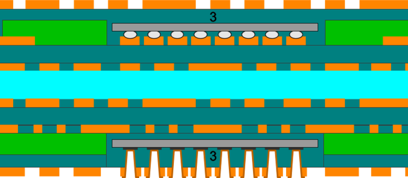
Now it is possible to create a cavity in the PCB and put the wafer or component in that cavity. You’ll see this done primarily with four-or-more layer boards. The typical process of making a circuit board involves making two layer boards, then bonding them together. If you have blind or buried vias, it’s necessary to have a drill stage before bonding those two boards together, which is why some PCB fabs don’t support it, and why prices increase with the number of layers.
With the embedded components process, the manufacturer cuts out the cavities necessary for the component in the appropriate layers (with a laser because the tolerance is so tight), then before the layer bonding process inserts the components inside, and closes it up. This works great for passives. 01005 components are like specs of dust, and in some cases it’s possible to sandwich the component between two layers without cutting a cavity, accepting an almost imperceptible bulge around the component.
To get the electrical conductivity between the component and the PCB, this can be done with bond wires for chips, or by soldering using normal (but much more precise) processes. There is some risk during later stages because this PCB will likely go through the reflow oven two more times for components on the top and bottom, possibly damaging the embedded component or breaking the internal connection. If the embedded component is connected by vias, the solder can wick into the cavity and cause shorts as well. In other words, it’s really hard to do, and requires tighter tolerances than most tools are capable of doing.
Considerations
This process demands precise equipment and adds a lot of steps to the PCB manufacturing process, and is therefore expensive. We already try to avoid blind and buried vias for exactly this reason, and embedded components are a similar problem with additional complexities. Expect that the price of your board will increase significantly, and that most factories aren’t going to be able to do it, and probably won’t want to invest in the equipment or expertise necessary to pull it off. There’s just not enough demand for it. You’ll also need to have EDA software capable of embedded component design like Altium, but none of the free ones have the feature yet.
More importantly, this may be a niche that will go away with newer technology, as custom ASICs are easier and easier to spin up. If you are spending lots of hours and dollars to make a smaller PCB, you may be able to accomplish the goal with a custom IC instead and make it even smaller with no embedded components at all. If only we could eliminate the need for a billion decoupling caps underneath a large BGA.


This came across my feeds last week. Murata has put the coil of a DC-DC converter between the PCB layers.
https://www.youtube.com/watch?v=CT3yCUjMXlc
What is this? A DC-DC converter for ants?!
Good thing there’s no relation between sex and electronics, otherwise things wouldn’t keep getting smaller. :-D
i invoke rule 34!
Porn … on an electron microscope
Looks like a hole in the video to me!
Oh I’m so happy someone got the title reference AND used another quote from the same same movie in the comments. Thanks, @gregkennedy for making my day.
Just for… Really really really really GOOD LOOKING people.
High power DC-DC bricks use this trick with custom designed ferrite cores that fit through and around the PCB:
http://www.mouser.com/ProductDetail/Delta-Electronics/Q48SC12042NRDH
“There’s cost and additional process, though, and requires a lot of coordination with the PCB fabricators and assembly houses.”
I imagine companies that do all this in-house would be the biggest market. I also image iFixit would probably give anyone who used this a low score.
iFixit doesn’t care about how the boards are made, only if they are available for purchase and easy to replace. Seems like they are more concerned with the physical construction of products. I get they are not to impressed with things like ram being embedded into circuit boards but that is because ram already has standards for expansion slots. I dont think that putting capacitors, resistors or diodes in between the layers is going to make much difference, as long as the board is easy to obtain and physically replace
And how about trace inductors? I have somewhere a DIY FM bug that uses copper trace as a coil and to keep board one-sided, the trimmer cap connects directly to the center end of coil…
http://www.we-online.com/web/en/leiterplatten/produkte_/ect/ect_uebersicht.php
I think this display is generally also with in PCB embedded LEDs: https://hackaday.io/project/10280-4-digit-charlieplexed-segment-display
“What’s really exciting is that components are now being embedded inside circuit boards.”
it is not exciting for me at all, but it surely will make pcbs completely unrepairable
As someone who repairs electronics for a living, I have to agree that this is the new peak of planned obsolescence.
This is what I was thinking while looking at it GREAT… Now Apple is going to have versions of their versions and the iDiots will pay them.
Thing is there would never would have never been affordable consumer electronics ever, to repair, if it where not for mass production made possible by the Industrial Revolution. Mass production is on track to taketh what it has giveth. Not sure how that can be avoided, without creating great hardship for all.
Affordable and economical are hugely different in this context. Repairable electronics was certainly more economical even if being a higher initial cost.
What makes iProducts affordable and economical is that it’s poorer nations like Africa and China where people including children pay with their health, quality of life and even death for the disposable products that marketing companies tend towards to maximize profits without any moral compass.
+1 RÖB
I may be an iDiot or am I? the $50 I paid for my 5C was subsidized by a two year contract, just like no contract plans subsidizes the cost of “Android” phones My 5C still works without having never been repaired, when those who have no contract phones may have paid up to six times what my 5C cost me so they had a working phone over two years by purchasing multiple phone whenever a bargain phone died. Mass production made possible by the industrial revolution created what is called planned obsolescence.. My take if mass production ended those bellyaching loudest about increased cost the loudest are those who are now belly aching about planned obsolescence now.
iDiot out…
First, similar contract (rate payment) plans exist for Android and for iPhones. I never wanted the “walled garden” or “golden cage” approach of Apple.
Second: Don’t think, that you really only paid $50, this is only the down payment, part of your monthly rate is paying for the rest of your phone’s cost. Only that you pay it for the whole length of the contracts run time, not only until you payed off the cost of your phone.
I did it different: I bought my Galaxy phone open without contract or provider special edition and have an extremely cheap contract. And it’s open, I already used Thai or Indian SIM cards when on holiday.
Can’t wait to see Luis ranting about it :D
Imagine a Thunderbolt power chip embedded in the board going bang.
Drill through the board and hope for a miracle.
Or burn it with fire.
The outcome would be the same but the satisfaction would be greater.
I bet you cursed the day integrated circuits were created…
Technological progress shouldn’t be slowed because people like to repair things (I do too) – there’s a difference between making things better/more compact and intentionally making things unrepairable.
No it’s not? And progress shouldn’t stop just because you make a living out some aspect of previous technology.
Naw, I’m sure there are other reasons to put a halt to progress. ;-)
Yah this looks bad even for recycling broken electronics so will make the ewaste problem even worse.
Totally, this is why I hate transistors. Even if a PC is built entirely from discrete transistors, you still can’t repair them, you have to replace the transistor. With the old tubes, you could get out the blowtorch and repair the tube.
The idea of trace inductors and capacitors is an old one. One of my earliest memories of an electronic device was a TV filter (probably a high pass filter to reduce ham radio interference) that was nothing but traces on a PC board. When I was older, my dad explained that they had made inductors and capacitors, forming an LC filter, using the PC board traces.
The filter was probably purchased around 1960.
A lot of very high current power supplies make current sensing resistors out of PCB trace, too. I have a Gould Biomation logic analyzer that has a 5V linear supply that is like 20A or maybe a little more. The current sense resistor is a serpentine-like trace half the width of my finger.
I was quite excited by this for high frequency switching of power MOSFETs as it would give the shortest and thus lowest inductance wiring. However the manufacturer we enquired with quoted greater than £10000 just to do some basic things. It’s a very complex process so I don’t think it will be cheap soon.
Lots of other PCB only components.
(Sp)ark gap for lightning protection.
Inductive pickups under a PCB motor used for feedback to the motor controller.
The four hacker PCB techniques that I like best are
1) Manhattan for RF circuits
2) Boards (Modules) on board with only a couple of extra components on the main PCB
3) Dead Bug!!
4) PCBs made into an enclosure
We’re getting closer to the technology used for the teleporter console board in the book version of “Battlefield Earth”. Terl makes a new board, starting with tracing out the circuit on the board then mounting components. He finishes it by applying an electrical charge that fries all the components.
They’re a ruse to fool any attempts to reverse engineer the board. The real circuit is what was drawn on the substrate. That’s protected by gas pressure inside the console and a trick screw with an internal fuse on the cover. To disassemble a console without blowing the real circuit, the console has to be put in an enclosure with the right type of gas, at the right pressure, Then the cover screws may be removed. Once properly opened, the console can be removed from the pressurized enclosure. IIRC they’re very rarely opened because there’s not much to the console aside from the main board and the external controls.
Until Terl was observed building the replacement board, and a Psyclo mechanic who knew the secret of how to open a console without destroying it revealed the trick, no non-Psyclo species was able to reverse engineer the technology. Sort of like the Harvey’s Casino bomb in 1980.
Quite a bit of clever stuff in that book, but it sure could have used a bunch of editing to slim it down 100 or so pages, or it could have been done as a trilogy.
My old copy says “Soon to be a major motion picture!” on the cover. Soon turned out to be 14 years after the publication date of that edition, and it failed to mention it would be a major failure.
Just looked it up in my worn copy (page 744 of 1066). For the real circuit, he first drew it on the board. Then he traced over the circuit with a tool that aligned all the normally insulating molecules into straight lines, making the traces conductive. Then he erased the drawn circuit leaving the featureless board with a now invisible circuit made of aligned molecules.
I’ve often wondered how I’d do a similar thing on transparent glass or plastic. The most obvious is probably by painting a circuit on using some transparent material like tin dioxide (SnO2).
Re the book, I recall it being an easy read and hard to put down. I think I read it twice and the second half (which isn’t in the movie) probably a few more times.
Did it get hot in here, or is that just the friction of Apple rubbing its non-repairable hands?
give it rest. Apple is not the only manufacturer of “repairable”/ difficult to repair consumer items. Hell they are far from being the first. I have had old timers tell me they found easier and more profitable lines of work when mass production, moved from point to point wiring to PCB.
They’re certainly carrying the flag at the moment, and giving it a rest will only make it worse. To make matters worse, other companies are looking at Apple, copying the troublesome design philosophy.
It might be unrepairable, but it allows for example for ultra-small buck convertors that go up to 3A in a 3x3x1.5mm package (TI TPS82130)
Interesting but not hardly worth all the hand wringing we are seeing. Shit even at this late of a date there are still those peeing and moaning over integrated circuitry.
Exactly. I’m more worried over the fact there are almost no (public at least) documentation of systems today, even if one can’t solder some blown transistors on a processor die one can simulate or emulate the processor given enough documentation.
Or implement it in FPGA.
Yah, I came to say something like this. First ICs and then surface mount were supposed to be the death of hobby electronics. Clearly they presented new challenges but also new opportunities and here we are today. Let’s not panic yet!
Frightening…
There’s no ‘irreparable’ – just different tools and a new skill-set to learn.
Of course that is in some way true (probably not when it comes to ICs) but the effort of removing several layers of glass reinforced plastics to reverse engineer a circuit is a bit more than needed otherwise. But that of course have to be done to reverse engineer any PCB with hidden layers at least to be sure (for analog circuits mostly).
But there’s something that have been used for a long time and is even worse to deal with: ceramic MCMs (Multi-Chip Modules). Imagine a PCB where each layer is made of an extremely hard material, then imagine that there can be hundreds of layers of conductors and components (resistors, capacitors, inductors) made using thin film techniques. There are often several thousands of external signaling excluding the wires going to the chips soldered to the surface of the module. That’s something hard to repair!
People work this way. At first everyone’s organs were just through-hole attached to their bodies. Then we got surface-mount organs and now technology has advanced so far that my heart is inside my chest.
High-end professional PCB manufacturers have been doing this for almost 20 years in various forms. It’s just new to hobbyists.
INSIDE the circuit board, you say?? neat article!
https://www.youtube.com/watch?v=TV3Oncvz_cU ;)
Hope hobby tech keeps up with this, lest we see the end of the hobby. Am only half-confident someone will come up with a workbench tech to let us play with it too.
Desktop millimeter radar to see into boards.
put b and w 35mm camera film or enlargement photo paper between case wall anti static pad. insert pad, insert device, move to a home next to an airport that uses back scatter x ray. buy a plane ticket, develop film when you get to your location . protip, fly to board makers house and beat them senseless with the case
Am I the only one thinking they just upped the game again on defcon badges?
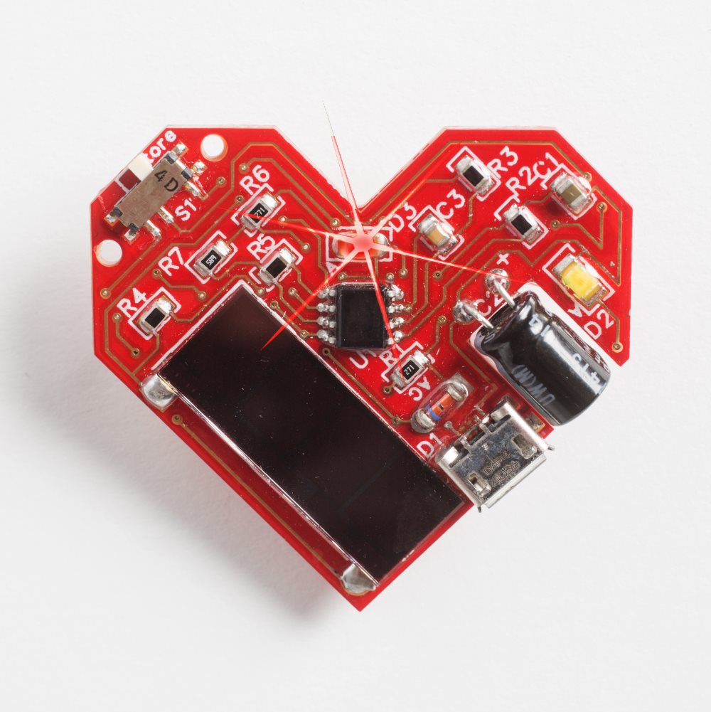
For all those worried about this being a game changer, relax. Embedded components is not new. Heck even the link in this article takes you to a 4 year old article. Embedded components have a purpose and in most cases, you won’t be hacking on a device using them anyhow. On the other hand, please consider the tricks of pseudo-embedded components (like the capacitor in the heart jewelry) for your projects as space utilization is one benefit that anyone can gain.