
You may have heard the phrase “flip-chip” before: it’s a broad term referring to several integrated circuit packaging methods, the common thread being that the semiconductor die is flipped upside down so the active surface is closest to the PCB. As opposed to the more traditional method in which the IC is face-up and connected to the packaging with bond wires, this allows for ultimate packaging efficiency and impressive performance gains. We hear a lot about advances in the integrated circuits themselves, but the packages that carry them and the issues they solve — and sometimes create — get less exposure.
Let’s have a look at why semiconductor manufacturers decided to turn things on their head, and see how radioactive solder and ancient Roman shipwrecks fit in.
The Old Packages
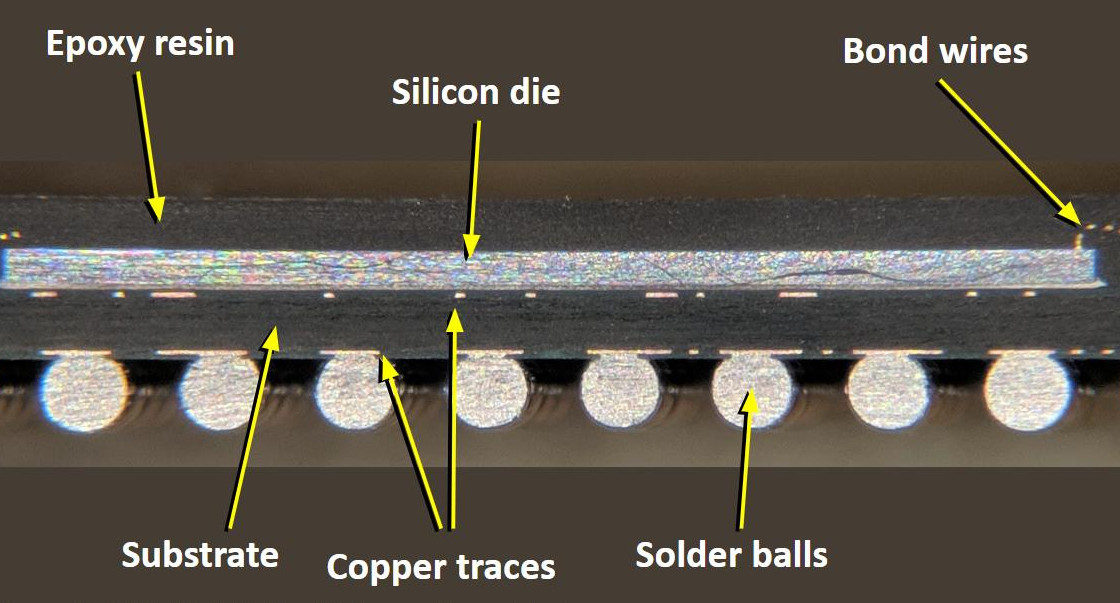
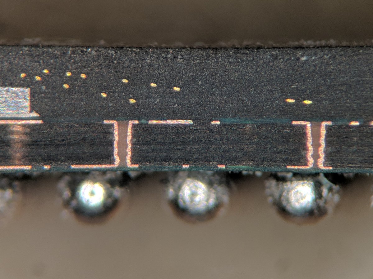
Very early integrated circuits were packaged in metal cans like the transistors of the day. Welded gold bond wires connected the die to the external pins. Open one of these old IC packages like a can of tuna, and the wires are plain to see. When DIP packages came about, they continued to use bond wires to connect the die to the IC pins, even though they were encapsulated in the plastic package.
This trend continued into surface-mount packages like SOIC, SSOP, and even BGAs, because it worked pretty well for parts from that period. But, as IC technology advanced, these packages became problematic. The first snag was the burgeoning size and complexity of the chips. As they grew, so did the number of connections required. Unfortunately, while the complexity grows with chip area, the number of possible wire-bond connections grows with the perimeter of both the die and the old-style packages. It’s X2 vs X, and at some point, there just isn’t enough space on the perimeter, so a more dense connection method had to be devised. A second problem was the performance of the wire bonds themselves. Like any conductor in free space, these little wires behave as inductors. This inductance can have serious consequences for high-speed circuits. As IC speeds increased, the inductance of the bond wires plus that of the package leads started to become a serious issue.
Flip Chips
A good solution to both problems is to turn the semiconductor die upside down. With the chip flipped this way, the connections can be made directly from the chip to the next layer below without any bond wires. This allows for more connections, since bond pads can be placed anywhere; there’s no need to restrict them to the periphery of the die. For pad-limited designs with many I/O connections, this can actually result in a smaller chip. Additionally, the connections can be made with a short, thick metallic bump, which has much less inductance (around an order of magnitude less) than traditional bond wires.
In some cases, flip chips connect directly to printed circuit boards using solder balls. In others, the die may be connected first to traces on a substrate, similar to an intermediate PCB, that then connects to the board itself. Traces on this intermediate layer connect the solder bumps from the die to the board connections. This allows for fanning-out connections on the die that would otherwise be too closely pitched for PCB connections.
While we may think of flip-chip technology as the new kid on the block, it’s actually been around for a long time. IBM pioneered the idea for discrete diodes and transistors in their mainframe computers of the 1960s, and it was later adapted for use in automobile electronics in the 1970s. Today, the technique is commonplace, and used in a wide variety of applications.
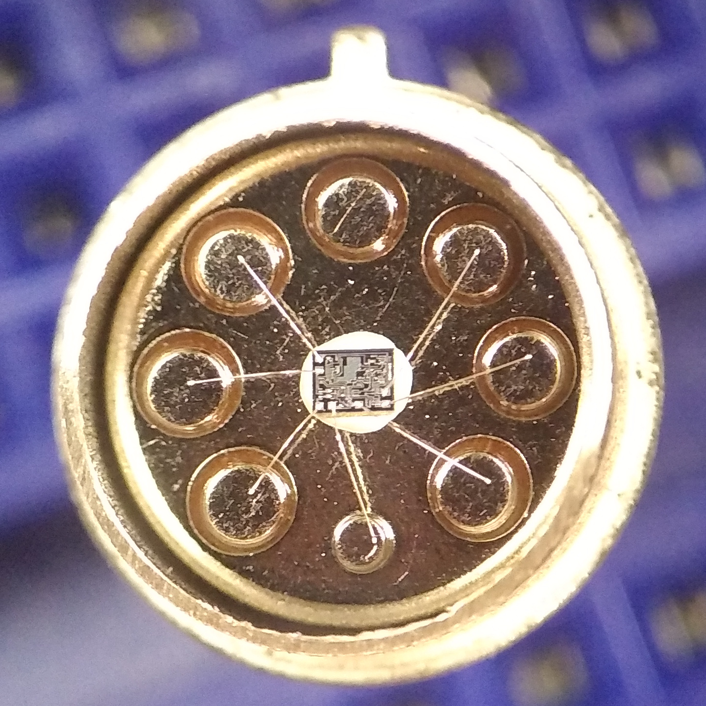
Not all leadless SMT packages have upside-down dice; there is a great diversity in IC packages. Some BGA packages use wire bonding, connecting the die pads to conductive traces on the package substrate before ultimately terminating in the solder balls on the bottom of the package. Likewise, the dice in QFN packages may be of either orientation. Sometimes the only way to know — just for curiosity’s sake — is to take a look inside the package.
Wafer-Level Chip-Scale Packaging
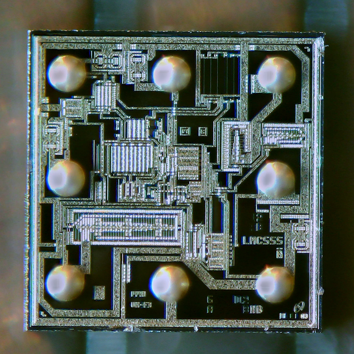
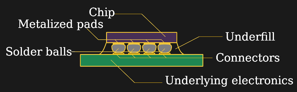
So, once you’ve decided to connect the die directly to the PCB, an interesting opportunity arises. You can turn the die into the packaging, and construct the whole assembly while the chips are still on the wafer. This is exactly what’s done in wafer-level chip-scale packaging (WLCSP). In this process, after the wafers have been manufactured, solder bumps are deposited on the bond pads, and an encapsulation coating is applied to both sides of the wafer. The now packaged chips, still on the wafer, are then tested and marked before being cut into individual units. This is a very efficient way to package the devices, and makes for a very efficient use of board space: since the package is the same size as the die, you just can’t get it any smaller.
While these chips are wonders of packaging efficiency, they can suffer some strange maladies. If you own a Raspberry Pi 2, you may be familiar with one of them. Shortly after its release, an interesting issue came to light when it was found that a bright flash (or a properly directed laser pointer) would interfere with the operation of a power regulator on the PCB, causing the Pi to reset. The chip in question was in a chip-size package with the die exposed below, and it turned out to be light-sensitive. Oops.
Maybe the most interesting problems with flip-chips, though, have to do with another sensitivity, specifically to alpha radiation.
Shipwrecks and Soft Errors
IBM first noticed in 1979 that their ceramic-DIP packaged DRAMs were susceptible to bit errors due to alpha particle emissions from the package lids. These alpha particles caused soft errors: one or more flipped bits with no damage to the hardware. Later, when flip chip packages became commonplace for complex ICs, soft error rates started to climb. The culprit: alpha particles emitted from tin-lead solder balls.
Alpha particles have very little penetrating power; a sheet of ordinary paper will stop them. Before flip chips, the packaging and even the silicon substrate itself provided adequate shielding, but when turned upside down, the sensitive side of the IC is now facing the solder. The resulting error rates could be alarmingly high. A Xilinx white paper from 2004, for instance, describes an issue arising from a packaging vendor incorrectly using high-alpha (i.e. “normal”) solder to assemble some of their flip-chip FPGAs, resulting in bit errors as often as every 230 hours of operation.
While we typically think of lead as a radiation shielding material, newly smelted lead is, in fact, slightly radioactive. Lead ore typically contains traces of uranium-238, which naturally decays (via a complicated chain) into a radioactive isotope of lead, Pb-210. Pb-210, in turn, eventually decays, with a half-life of 22 years, into Po-210, taking a brief stop as bismuth along the way. The final decay of Po-210 into stable Pb-206 releases an alpha particle, and that’s what causes the problems.
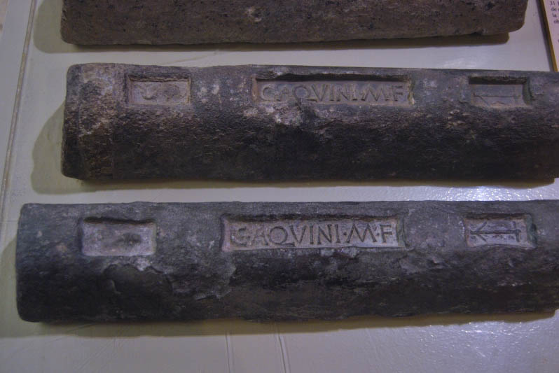
 Separating isotopes isn’t easy. This fact keeps nuclear weapons out of the hands of all but the few most powerful nation-states, but also makes it difficult to separate radioactive lead from the innocuous Pb-206. However, like most issues involving radioactivity, if you can wait long enough, the problem will go away by itself. Once the lead has been refined, the source of Pb-210 – the radio daughters of U-238 – is removed, and any existing radioactive isotopes begin to slowly cool off. After a few hundred years, very little alpha activity remains. So, one source for so-called low-alpha lead is metal that was refined in antiquity.
I remember around the turn of the century hearing about companies salvaging old lead from ancient shipwrecks to make low-alpha solder for vulnerable components, specifically the advanced microprocessors and FPGAs of the time. The lead was originally ballast or hull cladding, or carried as cargo, since it found use in an amazing variety of ways in ancient times – including plumbing for drinking water. Salvage companies would locate shipwrecks and other sources of ancient lead and scavenge it for use in sensitive electronic assemblies.
This practice would later become quite controversial as archaeologists grew concerned that valuable artifacts were being melted down, erasing cultural heritage. Although the headlines in 2013 were about physicists using ancient lead for neutrino experiments, by that time it was pretty clear that this isn’t a sustainable solution for electronic assembly. While some ore deposits are naturally less radioactive than others, and laser-based methods for isotope separation hold some promise, there aren’t really great solutions for economical low-alpha lead. For specialty applications where leaded solder is still required, alpha decay continues to be an expensive problem.
RoHS To The Rescue?
It would seem that with the RoHS directive, which mandates removal of the lead from solder, the alpha problem would be solved. Unfortunately, even at RoHS-allowed levels of contaminants, “lead-free” solders can still be hot enough to cause problems. In many cases, the activity of these so-called lead-free solders is due, surprisingly, to our old friend Pb-210. Lead is a natural contaminant in many metal ores, and tin sources may contain enough Pb-210 to cause problems for sensitive circuits, even when purified to “lead-free” solder standards. As a result, there’s an industry surrounding the production of low-alpha tin and RoHS-compliant solders, but of course, they aren’t cheap.
So, the next time you slap an IC onto a board, give a little thought to the package itself. And, if you’re seeing some strange behavior with your exposed-die part, consider your solder. You might just need some ancient lead.


This was an interesting read, i didn’t know that radioactivity was such a big problem for some packages.
I have very mixed feelings about WLCSP and stuff like this. On the one hand you can make really small electronics, process really high frequency signals and so on, but for a hobyist(??) it’s more like a nightmare. How do you solder it? And i don’t even talk about breadbording. Yeah, they might be some breakout-boards avaible, but still, not great for hobyists. I had do solder QFN recently, not fun.
When we started doing WLCSP chips, even some of the major manufacturers couldn’t manage them and had to get mezzanine boards made for them by those who could…
ECC.
ECC memory doesn’t save you if the bit in question is in a register (which is just memory) or the strike flips a gate somewhere in the data path. Memory is the most easily impacted component, but not the only.
There are a couple of processor architectures which avoid this by doing data checking throughout the data path, but they have not been all that popular. (latest SPARC for example).
The reason memory is the “most easily impacted” is primarily because the error is observable (it gets saved in the memory) plus memory is likely the highest density circuitry on a chip (better chance for the particle to hit something important). Other parts of the data path are affected, but it is difficult to capture one event that might happen every few days.
There’s some info that seems to be lost about ECC memory, regardless of whether it’s a hard or soft error: [1] Most ECC can only repair one bit [2] the longer memory is idle, the more likely it gets multiple errors in an ECC cell. These can be mitigated by continuous background memory “scrubbing” operations that simply read a cell and then the ECC correction takes action if a cell is corrupt. This is more complicated in today’s multi-core processors, as memory tends to be pushed to the max already. IBM has done a lot of seminal ECC work. TI’s Hercules dual-core ARM can be used as a lock-step processor (actually, clocks are slightly offset) with internal ECC flash and RAM memory.
Also, high altitude use of electronics can lead to more soft errors due to higher exposure to high-energy Cosmic radiation.
These same WLCSP ICs also have issues with camera flash or bright lights reflecting under and causing crashes too.
As for how to solder as a hobbyist. you can do it dead bug style for some, but mainly, you just hot air reflow it. I imagine a future where the beginner hobbyist starts with a reflow oven instead of a soldering iron.
instead of air reflow: https://hackaday.com/2010/10/15/vapor-phase-reflow-soldering/
The vapour creeps unter the chip between the solder balls much better than a flow of hot air.
“In some cases, flip chips connect directly to printed circuit boards using solder balls. In others, the die may be connected first to traces on a substrate, similar to an intermediate PCB, that then connects to the board itself.”
Interposer.
There’s no need for name calling.
I seem to recall that most of the initial alpha particle soft errors were due to “dirty” (e.g. radioactive) gold used in wire bonds and plated pads back in 1977 era. Back then, gold wires were ultrasonically (I believe) bonded to gold plated pads. The first “report” I recall reading that dealt with the topic was for a “state of the art” Mostek 4K (bit!) DRAM. I recall talking to an IC vendor back in 1978 who said: “our memory doesn’t do that” (i.e. have soft errors), so he definitely didn’t know what I was talking about. The Wikipedia article reference 2 on “soft errors” lists 1977 as the year alpha particle soft errors were initially detected. Back then, these chips were HUGE as were all their (tiny at the time), component parts, when compared to today’s devices. DRAMS used (still use?) high-resistance polysilicon resistors as loads to keep power dissipation low. This chips used much higher operation voltages and internal charges compared to today. One of the earlier fixes, BEFORE the radioactive gold was discovered, was to “passivate” dies with a polyimide coating. Most of this information is way too old for internet searches. Google needs to grab more old data books and digitize them (did ya read that Google?). There have also been instances of radioactive gold used in jewelry that resulted in finger amputations that held radioactive rings.
None of the gold isotopes are alpha emitters though? Gold 195 was a candidate for a weapon as its half life is relatively short and the fallout would be benign after a while.
As I said, this was a long time ago, and I don’t recall all the details, or if they were even given. There was no internet and easy data access, especially technical. I seem to also recall there was also radioactive “gold” (probably “dirty”) jewelry incident back in that time frame, and maybe some of that made it into the gold wire bond supply. I’m sure that all involved wanted to minimize blame and it’s accompanying financial risks. This era was when “routine” lithography used something like 5 um lithography rules, not the 6 nm of today. In my current perusals, I found an old NY Times article from 1983 about radioactive ceramic jewelry (from its Uranium glazing). Also, that Gold, Lead, Uranium, et al. are often found in deposits of pitchblende.
Here’s an NIH article on radioactive rings: https://www.ncbi.nlm.nih.gov/pmc/articles/PMC1451360/
A gold bond wire anecdote. A cousin worked at Micron Technology in Mountain Home Idaho in the 80’s. He told me about a guy who worked there in the chip fab and thought he’d found a way to get rich by stealing a spool of the gold bonding wire.
Took it to a pawn shop in Boise. Didn’t bother to melt it, left the Micron labeling on the spool. Of course the pawn shop called the police.
Cool article format. Reminds me of those old BBC tech shows that take you on a story and weave several topics together… like the Secret Life of Machines.
I’m surprised about the RoHS solders having too much lead though. The amount of lead in modern solders has been reduced by three orders of magnitude (RoHS limit is 1000ppm but typically SAC305 is 26 years. In that amount of time, the decay actually results in a lower chance of a bit-flip, so it’s actually much much less likely, no?
Not sure what happened to my comment. Re-posting because it was chopped up.
Cool article format. Reminds me of those old BBC tech shows that take you on a story and weave several topics together… like the Secret Life of Machines.
I’m surprised about the RoHS solders having too much lead though.
The amount of lead in modern solders has been reduced by three orders of magnitude
(RoHS limit is 1000ppm but typically SAC305 is 26 years.
In that amount of time, the decay actually results in a lower chance of a bit-flip, so it’s actually much much less likely, no?
Sorry, I guess is it the greater-than, less-than symbols that chopped up my comment?
Cool article format. Reminds me of those old BBC tech shows that take you on a story and weave several topics together… like the Secret Life of Machines.
I’m surprised about the RoHS solders having too much lead though. The amount of lead in modern solders has been reduced by three orders of magnitude (RoHS limit is 1000ppm but typically SAC305 is 200ppm) so the probability of a bit flip is now basically nil. If an EXTREME case before would see an average bit-flip occurring every 230 hours, it’s now 26 years. In that amount of time, the decay actually results in a lower chance of a bit-flip, so it’s actually much much less likely, no?
The end of the article should have stated next time you try to solder anything on a board, regardless of the chip package, first and always first, GROUND YOURSELF BEFORE YOU DO ANYTHING.
because it seems like the error in which occur as mentioned in the article seems if those individuals are not properly following procedures on IC work.
Additionally,
I find the article stating the LEAD FREE from ROHS is incorrect. The allotted amount of hazardous materials was limited. The presence of some of the allotted materials do exist. For most non ROHS items,
the MILITARY will be the one using those items due to the stability of those components.
I’m sorry but I don’t believe you that Brian was the one to discover the Antikythera mechanism.