FPGAs are awesome — they can be essentially configured into becoming any computing device you want. Simply load your selected bitstream into the device on boot, and it behaves like a different piece of hardware. With great power comes great responsibility.
You might try to hack a given FPGA system by getting between the EEPROM that stores the bitstream and the FPGA during bootup, but FPGA manufacturers are a step ahead of you. Xilinx 7 series FPGAs have an onboard encryption and signing engine, and facilities for storing a secret key. Once the security bit is set, bitstreams coming in have to be encrypted to protect from eavesdropping, and HMAC-signed to assure that they are authentic. You can’t simply read the bitstream in transit or inject your own.
Researchers at Ruhr University Bochum and Max Planck Institute for Cybersecurity and Privacy in Germany have figured out a way to use the FPGA’s own encryption engine against itself to break both of these security guarantees for the entire mainstream 7-series. The attack abuses a MultiBoot function that allows you to specify an address to begin execution after reboot. The researchers send 32 bits of the encoded payload as a MultiBoot address, the FPGA decrypts it and stores it in a register, and then resets because their command wasn’t correctly HMAC signed. But because the WBSTAR register is meant to be readable on boot after reset, the payload is still there in its decrypted form. Repeat for every 32 bits in the bitstream, and you’re done.
Pulling off this attack requires physical access to the FPGA’s debug pins and up to 12 hours, so you only have to worry about particularly dedicated adversaries, but the results are catastrophic — if you can reconfigure an FPGA, you can make it do essentially anything. Security-sensitive folks, we have three words of consolation for you: “restrict physical access”.
What does this mean for Hackaday? If you’re looking at a piece of hardware with a hardened Xilinx 7-series FPGA in it, you’ll be able to use it, although it’s horribly awkward for debugging due to the multi-hour encryption procedure. Anyone know of a good side-channel bootloader for these chips? On the other hand, if you’re just looking to dig secrets out from the bitstream, this is a one-time cost.
This hack is probably only tangentially relevant to the Symbiflow team’s effort to reverse-engineer an open-source toolchain for this series of FPGAs. They are using unencrypted bitstreams for all of their research, naturally, and are almost done anyway. Still, it widens the range of applicability just a little bit, and we’re all for that.
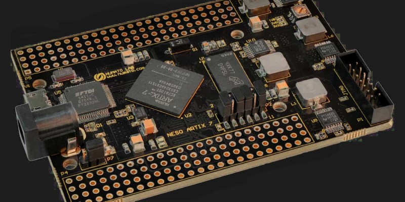
[Banner image is a Numato Lab Neso, and comes totally unlocked naturally.]


Well, how theturntables…
…or in German “Da hat sich die Wendung aber geblättert” (Doesn’t make much sense either…)
Zu tief ins Glas geschaut?
This is a rather clear design oversight…
Wouldn’t be all that hard for Xilinx to fix in their next generation.
Ie, if the authentication is wrong, then it should scrap the contents of the register as well.
Though, would be nice if FPGA manufacturers had more free development tools that didn’t have frankly obtuse licenses….
At least for the lower end devices. Sometimes a small FPGA is a nice solution to a problem. But I haven’t found any FPGA vendor that seems sensible.
At least the big 3 all have free tools for lower end devices and don’t seem to have any more complex licenses than any other company
For me Lattice did the trick, and so far I’m not regretting leaving Xilinx for them.
Same
Then you need to use microsemi igloo chips for your project. The software is for free.
The best is that the chips use flash programming, that means that they do not have a bit stream from a memory chip that you can hack.
Yep, they did fix it. UltraScale and UltraScale+ devices dont have this vulnerability (they’re the successor to 7-series.
Thanks for the write up, it makes it all the more clear the impact. When I first saw mention of it elsewhere it didn’t seem as exploitable as the write-up here makes clear.
They used the FPGA to destroy the FPGA
And in the end, you get… An obfuscated, non documented bitstream. Great, but until there’s a clear documentation of the bitstream and/or a tool reverse it to a netlist or better a VHDL/Verilog code, it’s only useful for… copiers of the PCB/system for example.
still going to cause a “brown pants” alert for some who thought the encryption was unbeatable (yes, I know, foolish)
A lot of high-end military HW uses FPGAs (because there is little regard to the cost) for example…
A lot of the high tech vertical applications (including military, financials institutions etc) use it because there might not be an off the shelf that fits their requirements. Sometimes you got to throw hardware at a problem because software bottleneck.
Individually the FPGA seems expensive. When you look at the high R&D cost+time for chips for very low volumes (vs rest of industries) , FPGA come out an alternative.
Making low volumes ASICs are indeed very expensive.
And if 2 months after making the chips one realizes that it has a flaw, well remember all that money one recently poured into making said chips?
Not to mention, there isn’t just chip production, one also got to make the photomasks, and they alone costs a lot of money.
Then there is all the waiting in line for factory time… Unless one owns the fab oneself, waiting anywhere from 6-24 months isn’t unheard off. (A lot of projects jumps in line before even starting chip design itself.)
So FPGAs can actually be more expensive than an ASIC solution and still be the more cost effective option. Since it competes against a solution that needs tons of time, money and a high risk of needing to be redesigned and spend yet more time and money on it….
ASICs though have a large speed and power efficiency advantage. Not to mention being able to be optimized heavily to one’s application. So sometimes one has no other option than an ASIC. Since FPGAs are in fact having rather low performance for their price, and especially for the power they need, not to mention usually not being all that suitable for analog/RF applications. (FPGA’s can though still have DACs, ADCs, analog Switches, RF frontends, etc. But it isn’t always as applicable as one might want it to be.)
But the strongest advantage of FPGAs are their immense flexible due to being programmable, so they can make up for a lot of their deficits in a lot of applications. Not to mention their usually fast turn around time compared to ASICs. (Literally, we can order an FPGA on Friday, make our code over the weekend and program the chip on Monday and show it on a board to our colleges by lunch. Larger FPGAs might take more time though, but relatively speaking, it is still very fast.)
No, that’s only half of the paper. And, to be honest, the idea that the bitstreams are “obfuscated and non-documented” is… a little naive. They’re obfuscated and non-documented in the “not open source” sense. To anyone with resources, it’s pretty straightforward to reverse. Extracting the block RAM contents is extremely easy.
The *other* half of the paper, which the article doesn’t mention, is that they also give a mechanism for signing any bitstream of *your own*. Which means that literally any 7-series hardware is now hackable.
Emulate the FPGA on a much faster system so it can reboot at warp speed to cycle through the bitstream quicker. Wouldn’t need to emulate the entire FPGA, just the parts involved in this process.
If you had the information necessary to emulate the encryption engine (i.e. the secret key), you wouldn’t need to do this in the first place…
Anyone who wants to protect their IP wouldn’t leave debug pins available on a final product. Good luck getting to those on a 600+ ball BGA.