

It seems fair to say that semiconductor technology has been one of the most influential inventions in human history. Practically overnight it turned human technology from being large, cumbersome and power-hungry into an increasingly sleeker, more power-efficient and much more capable form. It has become practically impossible at this point to imagine modern society without semiconductor technology.
That said, we didn’t always use today’s silicon-based semiconductor technology, and although silicon-based semiconductors are exceedingly versatile and adaptable, they do have their limitations. The past years we have seen for example gallium-nitride semiconductors make big inroads in power switching technology, and more exotic forms like diamond-based semiconductors keep making their tantalizing appearances.
In this article we’ll take a look at how we ended up at silicon as the default for semiconductor technology, as well as why we may want to consider moving to other materials.
Semiconductors
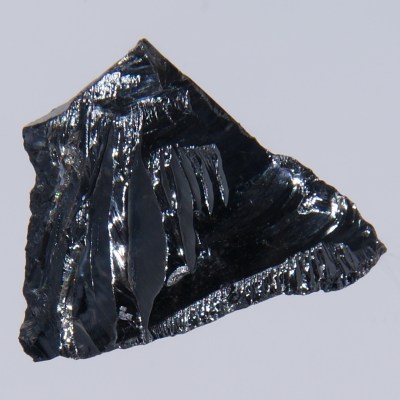
Although semiconductor technology works on very different principles than vacuum tubes and relay-based electromechanical systems, ultimately the goal is the same. This being to make electrons go to certain place when and where you want them to go there. In the case of semiconductors this is achieved through n-type and p-type materials, which are areas in the semiconductor material which display different electron mobility behavior.
The base material is – as the name suggests – a material that falls in between a conductor and an isolator. This conductivity can further be altered by embedding other elements into its crystal matrix, which is generally called ‘doping’. This creates an extrinsic semiconductor, as opposed to the pure, undoped intrinsic semiconductor. This doping process create two distinct types of semiconductor, being the aforementioned n- and p-types.
These letters refer to whether they hold a negative or positive charge, effectively whether this semiconductor material is an acceptor (p-type) or a donor (n-type) of electrons. It’s not required to dope the base material to create both n- and p-type areas, which led to many variations just within the metal-oxide-semiconductor (MOS) family, including the n-type MOSFET-based NMOS, p-type MOSFET-based PMOS and the complementary CMOS that uses both types.
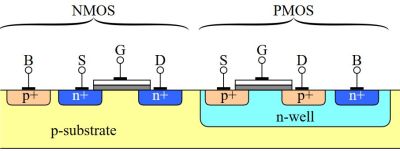
CMOS became the dominant technology by the 1980s to create field-effect transistors (FETs), although the ‘MOS’ part isn’t necessarily technically correct any more as the original aluminium layer can be replaced with polysilicon.
Of course, semiconductor technology didn’t start right off the bat with today’s silicon, dopants and construction methods. The first functional transistor and diode designs are good examples here of where the revolution began, and how things evolved from there.
The First Diode
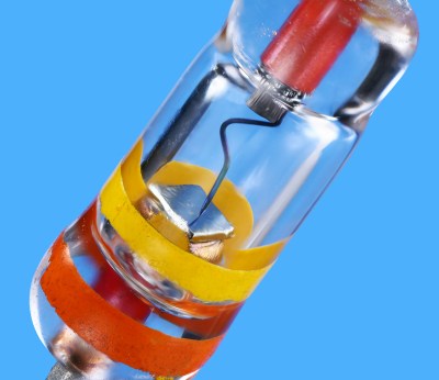
Although the invention of the point-contact transistor in 1947 is pretty well-known at this point, semiconductor diodes came onto the scene first. The first crucial discovery here was made by German physicist Karl Ferdinand Braun in 1874, when he discovered the asymmetric conduction of electricity in a range of materials involving a metal-semiconductor junction between a metal and types of minerals.
The discovery of this type of junction laid the groundwork first for a practical point-contact diode by the 1930s, using semiconductors ranging from selenium and silicon carbide to germanium and silicon. These were found to be much superior to the thermionic diodes that were first put into commercial use. Especially the push to develop radar and radio technologies during World War 2 drove the development of better semiconductor diodes.
With increased understanding of doping the intrinsic semiconductor material to affect its behavior, it was thus only a matter of time before the point-contact transistor was developed. From there both practical experimentation and a deeper understanding of the underlying electron mobility principles drove innovation forward.
Silicon As Easy Mode
The primary reason why silicon is the most-used semiconductor material today has less to do with it being a good base material and more with it being both plentiful, cheap and easy to process. The silicon dioxide (SiO2) that forms the pure silicon crystals is the main constituent of sand where it’s called quartz. It will readily melt and can be drawn into very large crystals that can subsequently be cut up into the silicon wafer on which semiconductor circuits can be etched.
Silicon’s band gap is however rather small at 1.14 eV, which means that the correct functioning of circuits created with this semiconductor will cease much sooner with higher temperatures including those generated by the device itself. So-called wide-bandgap semiconductors have a bandgap of >2 eV, which includes the gallium-nitride (GaN) semiconductor which the past years has become a frequent sighting in compact power electronics where being able to run hotter without issues and higher efficiency is considered a big selling point.
GaN’s bandgap is 3.4 eV, which puts it pretty high up in the bandgap rating. In addition to a higher bandgap number, its thermal conductivity is also pretty good at about 230 W·m−1·K−1. These advantages makes it economically feasible to produce GaN components despite the material being harder to process. Which is also the crux of why diamond semiconductors haven’t yet cornered the market.
Before moving on, an interesting note is that germanium has one advantage over silicon despite having an even smaller bandgap. This being that it doesn’t have to be as extremely pure as silicon to work well, which was a benefit especially during the early days of semiconductor technology.
Peak Semiconductor

Although diamond isn’t necessarily the ultimate semiconductor material, its properties makes it look very good indeed. With a bandgap of about 5.6 eV and a thermal conductivity of 900–2,320 W·m−1·K−1 it pretty much destroys both silicon and GaN. The only problem we are facing here is that diamond is an absolute pain in the backside to create large wafers from, not to mention dope the crystal lattice without using the easy ion implantation used for silicon wafers.
Creating diamond wafers requires growing them from seed crystals, rather than just drawing a massive crystal from a vat of molten goo as in the case of silicon. This alone is highly problematic for any large-scale commercialization.
The issue of doping and similar typical semiconductor circuit things being rather hard with diamond is not unique to silicon semiconductor alternatives, which is one reason why the MESFET field-effect transistor was developed. This drops the insulating oxide layer under the gate, instead using a metal-semiconductor (Schottky) junction.
Such a MESFET design allows for other exotic semiconductor materials like gallium arsenide and silicon carbide, the latter being rather comparable to GaN in terms of bandgap and thermal conductivity, while allowing for very high switching speeds.
An Exciting Future
Despite the occasional bouts of doom-and-gloom stories about the semiconductor industry and issues with scaling and cooling, semiconductor materials like diamond show that there’s still a lot of potential to look forward to. Diamond-based semiconductors could potentially outperform all currently used commercial semiconductor materials, while rapidly moving any waste heat away to whatever cooling solution exists.
Even before said Diamond Age commences, the rise of silicon alternatives like GaN are already showing that despite many decades of breakneck innovation we are hardly at the pinnacle of what is possible. Although making predictions about the future is a fool’s errand at the best of times, it’s good to remain optimistic about such potentially world-changing events like the death of silicon semiconductors in favor of something much better.











Please be kind and respectful to help make the comments section excellent. (Comment Policy)