Modern video games are nothing short of amazing. My son and I were playing through the one of the latest Zeldas, which involve a mix of combat and puzzle-solving that’s pretty much the hallmark of the franchise. But the most recent open-world Zelda is simply massive. Made by around 1,000 people at a development expense of $150,000,000, it takes probably 60-80 hours to play through if you’re not rushing, and more if you’re taking it easy. It has layers of game mechanics, and worlds in the sky, on land, and underground. It’s big in every way.
Contrast the games of my youth, which were a lot smaller. Written by a pair of people or maybe a handful, with playtimes in the single-digit hours, and of course fitting in the limited computing resources of the time. But the low-stakes nature of the early phases of the industry meant that software developers could take risks, and many of the games were consequently kinda idiosyncratic in this more innocent time.
I think there’s something to be said for small games. They don’t require a lifestyle commitment just to get through. They can still be fun, without taking all of your time. And honestly, when you’re done with a game quickly, you have more time for other stuff. Granted, some of this spirit lives on in the small indie games of today, but even so, game developers have the big studios’ products in the backs of their minds when they are working on their smaller oeuvres.
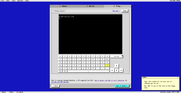
We were talking about preserving old games for posterity around Hackaday and on the podcast, and our conversations reminded me of a couple of educational games that, despite their rudimentary graphics, are still pretty good today. Both were electronics related, and both are still playable today thanks to efforts on emulation and software preservation. To get a feel for the 1980’s, give Rocky’s Boots a try. (I like the TRS-80 Color Computer version the best, but that may just be nostalgia.) Most of you grownups out there will get through it in an hour or so.
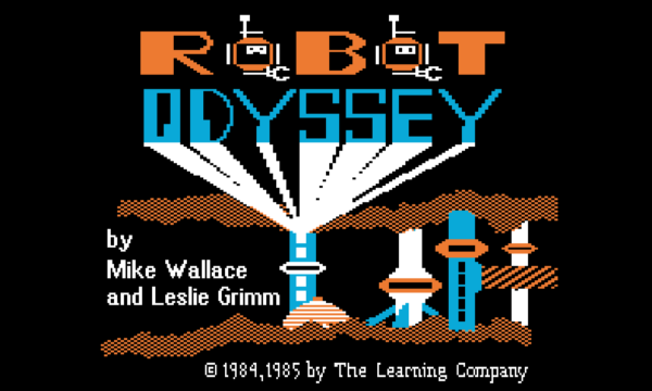
And if you want a challenge, try Rocky’s harder sequel: Robot Odyssey. If you already have a background in digital circuits, you’ll find it doable. Younger me hit a wall about two-thirds of the way through.
Both of these games stick with me because they taught me something, but also because they were simply quirky in a way that a game can only be when it’s written by a small team of folks who are just having fun programming it. If you pitched “a puzzle game about a raccoon who builds logic circuits to activate robot boots”, the boardroom would look at you like you’re out of your mind. But it’s just exactly the quirkiness and individuality of some of these early games that I cherish the most.
If you find yourself knee-deep in an endless modern game, take a side-quest off into a more naive time, and you’ll appreciate why people are putting efforts into archiving them.