Fail Of The Week: Unconnected Nets In KiCad

fotw-unconnected-net

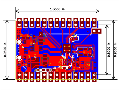
From the title and the image above you surely have already grasped this Fail of the Week. We’ve all been there. Design a board, send it to fab or etch it yourself, and come to find out you’ve missed a connection. Automatic checks in your software should prevent this, but when making small changes it’s easy to overlook running the checks again. This is exactly what [Clint] did with this board; leaving a net unconnected in the schematic, which made its way through to the board layout and into the OSHPark boards.

Okay, so fix it with jumper wire which is clearly what he did (white wire in the lower left image above). But since this is rev3 of his PCB it’s pretty upsetting that it happened. The meat and potatoes of the fail is the missing software feature that led to it. KiCad doesn’t have a pin swap tool in the board layout. Really? We use KiCad frequently and didn’t realize that the feature was missing. Needing to simplify his board layout, [Clint] went back to the schematic to swap some resistor network pins by hand. He pushed the change through the netlist and into the board layout, not realizing he had left an input gate unconnected.

A bit of searching proves that pin swapping may be coming to KiCad soon. It’s on the CERN roadmap of features they plan to add to the open source PCB layout software. We remember hearing about CERN’s plans quite a while ago, and thought we featured it but the only reference we could find is [Chris Gammell’s] comment on a post from back in December. It’s worth looking at their plans, these are all features that would make KiCad a juggernaut.

EDITORIAL NOTE: We’ll soon be out of story leads for this series. If you have enjoyed reading weekly about fails please write up your own failure and send us the link. Of course any documented fails you find around the internet should also be sent our way. Thanks!


2013-09-05-Hackaday-Fail-tips-tileFail of the Week is a Hackaday column which runs every Wednesday. Help keep the fun rolling by writing about your past failures and sending us a link to the story — or sending in links to fail write ups you find in your Internet travels.

A Low Cost Dual Discriminator Module For The Easy-phi Project

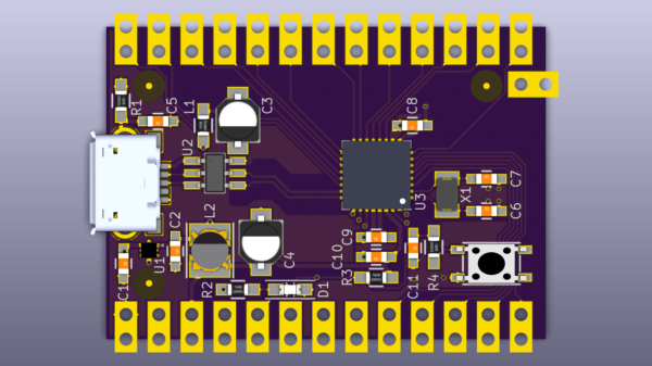
A few months ago I presented you the Easy-phi project, which aims at building a simple, cheap but intelligent rack-based open hardware/software platform for hobbyists. With easy-phi, you simply have a rack to which you add cards (like the one shown above) that perform the functions you want.

Recently my team finished testing our FPGA-based discriminator or “universal input” if you prefer. As easy-phi cards use a well-defined electrical signal to communicate with each other, we needed to make a card that would translate the different kinds of electrical signals from the outside, as well as perform plenty of other functions. It was therefore designed to have a 100MHz input bandwidth with an AC/DC coupled 50 ohm/high impedance input stage (x2) and 4 easy-phi outputs. For this module, we picked the (old) spartan3-an FPGA to perform the different logic functions that may be needed by the final users (high speed counter, OR/XOR/AND, pulse creation,…). Using the cortex-m3 microcontroller present on the board, it may be easily reconfigured at will. All design resources may be found on our Github, and you can always have a look at our official website.

KiCad Video Series: From Concept To Manufacture

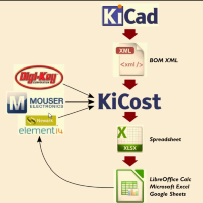
Many of our readers took the habit of using Eagle to design their PCBs. Even if you’ll find plenty of support for this software as well as a lot of parts libraries, the software comes with limitations. The useable board area is limited to 4×3.2 inches, only two signal layers can be used and more importantly the schematics editor can only create one sheet. On the other side, some of you may already know KiCad, a free open source and unrestricted schematics and layout software. [Chris] just tipped us of a video series he made, showing people how to design and build their very first PCB using this software. It’s a simple 555 circuit, but goes through all the steps necessary to design a PCB that costs only $5 through OSHpark… and will blink by the end. All the videos are also embedded after the break.

Continue reading “KiCad Video Series: From Concept To Manufacture”

Easy-phi: An Open Source Platform For Experimenters

As a few of Hackaday readers may already know, my day job involves working with high speed electronics. For the last few months, my team at [Université de Genève] in Switzerland has been working on an open source platform (mostly) targeted for experimenters: the easy-phi project. The main idea is to build a simple, cheap but intelligent open hardware/software platform consisting of a 19″ frame (or smaller), which can house a big variety of electronic modules. Hobbyist would therefore only make/buy the modules that would suit their needs and control them through a web page / standalone application / Labview module.

I detailed in more depth on my website the technical aspects of the project. To give you a quick and simple overview, the rack is essentially a USB hub that connects all the modules to a Cubieboard. It also integrates a few synchronization signals, a clock and a monitoring system for voltages, temperatures, power consumption. The modules are made of template + module specific electronics. The template electronics are part of the ‘easy-phi standard’, they consist of the Arduino compatible SAM3X8E microcontroller and of a few other power related components. This ensures electrical and firmware compatibility between the rack and modules that you guys may develop. It is important to note that the modules are enumerated on the USB bus as composite CDC (communication device) and MSC (mass storage). The CDC is used to configure the module while the MSC allows you to grab its documentation, resources, and standalone application in case you use the module without the rack.

The chosen schematics / layout software is Kicad, and all current files can be found on our github. Others will be uploaded once we have tested the other modules currently in the pipe. As the ones we’re developing are physics oriented, we hope that enthusiasts will bring easy-phi to other domains. Don’t hesitate to contact us if you have any question or if you’d like to contribute.

Creating Irregular Board Outlines In KiCad

irregular-borders-in-kicad

One of the benefits of plain text file format is that you can go in and edit them by hand. This is part of the KiCad board outline hack which [Clint] wrote about in a recent post. He wanted a unique board outline, which is something that KiCad isn’t necessarily well suited for. His solution was to create the outline as an image, then import it. If you’re wondering what custom shape is called for this type of work we’d like to point you to the (kind of) bottle opening HaDuino. That PCB layout was done on Eagle, which has a bit more leeway with special shapes.

Before getting to the code editing step seen above [Clint] used the built-in feature for KiCad that will turn an image into a component. He exported that code and altered it using a text editor in order to change the layer setting for the shape to that of the board outline. This took him from a plain old image, to a module which can be selected and dropped into the board editing program. It’s a snap to do this sort of thing for the copper layers too if you’re interested in using your mad graphics editing skills to layout an art piece on copper clad.

Turning PCBs Into Art

Designing a circuit, laying out a board, and sending it off to be fabbed is so easy anyone can do it. A lot of people are, in fact, and with the traditional tools like KiCAD and Eagle, a lot of different boards look very, very similar. You could always add some cool silkscreen graphics to your board to make it stand out, but [Saar] has a better solution: it’s called PCBmodE, and it allows you to draw circuits artistically instead of the 45° angles we’ve become so accustomed to.

PCBmodE takes the parts, pads, signals, and vias for boards stored in JSON files and converts them to an SVG representation. The file is then routed (manually, but [Saar] is working on automated routing) and Gerberized so it can be sent off to a production house.

You can grab PCBmodE over on bitbucket, but right now it’s still a very early version. Vias and copper pours are working, but [Saar] has only fabbed this board so far.

Assigning New Packages To Eagle PCB Components

adafruit-eagle-component-creation-tut

If you’ve spent any time at all laying out your own circuit boards we’re sure you’ve run into the issue of not having the right component or package available in the standard libraries. If it’s a common part, chances are the symbol definition will be there.  But perhaps the footprint you want to use is missing? Here’s an easy to follow tutorial which demonstrates how to assign new packages to existing Eagle PCB components. It even shows the basics of how to tweak the footprint to fit your needs (like making SMD footprints easier to hand solder).

This will not teach you how to make your own custom symbols, or how to build packages from scratch. But it will let you locate the package you want to use from a different component, then copy it to your own library for use with different parts. And the techniques shown make this a quick and relatively painless process.

We certainly don’t want to start another comment quagmire like the recent PIC v. AVR discussion. But we’ve used both Kicad and Eagle rather extensively and feel that neither one has really mastered part/footprint creation in a user-friendly way. We like Kicad’s total separation of footprints from components, and it’s myriad of parameters which can be used to tweak the layout. But if you use the same components frequently, Eagle’s standard of linking parts and footprints does end up saving a lot of time. What do you think?