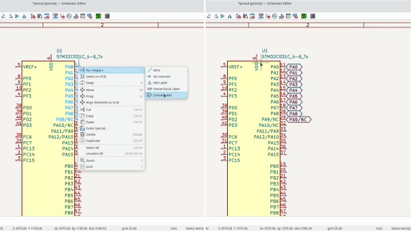
An image showing the new KiCad feature that allows you to easily generate schematic labels from IC symbol pin names

KiCad 8 Makes Your Life Better Without Caveats

A few days ago, KiCad 8 was released, and it’s a straight upgrade to any PCB designer’s quality of life. There’s a blog post as usual, and, this year, there’s also a FOSDEM talk from [Wayne Stambaugh] talking about the changes that we now all get to benefit from. Having gone through both of these, our impression is that KiCad 8 developers went over the entire suite, asking: “this is cool, but could we make it better”? The end result is indeed a massive improvement in a thousand different ways, from small to fundamental, and all of them seem to be direct upgrades from the KiCad 7 experience.

Continue reading “KiCad 8 Makes Your Life Better Without Caveats”

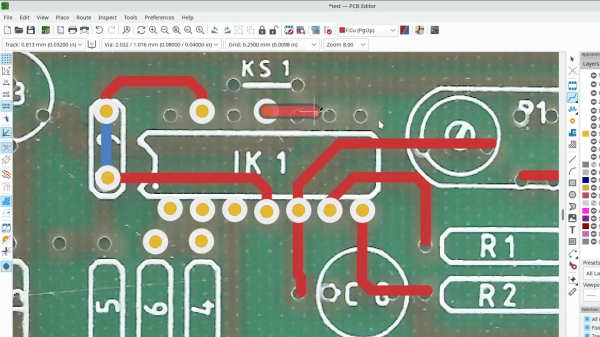
Screenshot of KiCad 7 feature that lets you overlay a PCB bitmap image and draw traces over it, being used for board reverse-engineering purposes

KiCad 7.0.0 Is Here, Brings Trove Of Improvements

Yesterday, the KiCad team has released KiCad 7.0.0 – a surprise for those of us who have only gotten used to the wonders of KiCad 6, and it’s undoubtedly a welcome one! Some of these features, you might’ve seen mentioned in the KiCad 2022 end-of-year recap, and now, we get to play with them in a more stable configuration. There’s a trove of features and fixes for all levels of KiCad users, beginners, hobbyists and professionals alike – let’s start with some that everyone can appreciate! Continue reading “KiCad 7.0.0 Is Here, Brings Trove Of Improvements”

KiCad 2022 Year End Recap

KiCad 2022 End-of-Year Recap And 7.0 Preview

[Chris Gammell] moderated the KiCad 2022 End-of-Year Recap with several KiCad developers and librarians. They reviewed what’s been bubbling up in the nightly KiCad 6 builds, what we can expect from KiCad 7, and even answered some questions from the user community. Over the course of 2022, the KiCad project has grown both its development team and library team. The project even has a preliminary support commitment from the CERN Drawing Office!

Improvements to the KiCad Schematic Editor include smart wire dragging that simplifies moving components around within schematic diagrams. Components selected in the schematic now remain selected while switching to the PCB Editor. Internal documentation of schematics has advanced with support for fonts, embedded graphics, and the inclusion of hypertext links to datasheets and other reference materials. New features for PDF generation offer interactive files and links between sheets.

A new search panel within the KiCad PCB Editor supports finding components by footprint, net, or text search. A property panel allows common properties to be edited across multiple selected items. While a full-blown auto-router remains outside of the scope for KiCad, “push and shove” routing is faster and easier. An “attempt to finish” feature routes a quick connection for the currently selected trace, and “pack and move” positions all selected footprints into proximity to simplify placing them as neighbors within the board layout.

The KiCad PCB Editor also adds support for the use of fonts and inverted “knockout text” which even works on copper zones. Bitmap graphics can be imported and scaled beneath layout work as reference illustrations. Private footprint layers can be used to place extra documentation within footprints. The design rule checker (DRC) now can catch more layout issues, especially those that may impact manufacturability.

These are just a sampling of the impressive improvements we can expect with KiCad 7.0. There are also additions to circuit simulation and modeling features, a new command line interface for script-based automation, ARM64 support for KiCad running on Apple silicon, and a huge number of additions to the default library including symbols, footprints, and 3D Viewer models.

The KiCad team suggests several ways to support the project. There are always needs for additional developers and librarians. Financial contributions can be made at kicad.org. As users, we can run the nightly builds, try to break them, and give feedback in the form of detailed bug reports. Community testing will help make KiCad 7.0 as solid as possible. The project team is also seeking open hardware projects to include with KiCad 7.0 as demos.  For example, the StickHub project was included with KiCad 6.0 as a demo.

The official release of KiCad 7.0 is currently scheduled for January 31, 2023. While we wait, let’s flashback to our January 2022 presentation of what features made it into the KiCad 6.0 release.

Continue reading “KiCad 2022 End-of-Year Recap And 7.0 Preview”

Avoiding PCB Crosstalk

Now that it is relatively cheap and easy to create a PCB, it is a common occurrence for them to be used in projects. However, there are a lot of subtleties to creating high-performance boards that don’t show up so much on your 555 LED blinker. [Robert Feranec] is well-versed in board layout and he recently highlighted an animation on signal crosstalk with [Eric Bogatin] from Teledyne LeCroy. If you want a good understanding of crosstalk and how to combat it, you’ll want to see [Eric’s] presentation in the video below.

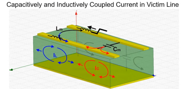
Simplifying matters, the heart of the problem lies in running traces close together so that the magnetic fields from one intersect the other. The math is hairy, but [Eric] talks about simple ways to model the system which may not be exact, but will be close enough for practical designs.

Continue reading “Avoiding PCB Crosstalk”

Inductance In PCB Layout: The Good, The Bad, And The Fugly

When current flows through a conductor it becomes an inductor, when there is an inductor there is an electromagnetic field (EM). This can cause a variety of issues during PCB layout if you don’t plan properly, and sometimes we get burned even when we think we have planned for unwanted inductance and the effects that come with them.

When doing high speed logic we need to be able to deliver sudden changes in current to the devices if we want to have proper switching times and logic levels. Unfortunately inductance is usually not a friend in these circumstances as it resists those sudden changes in current. If the high speed devices are driving capacitive loads, which themselves are resisting changes in voltage, even more instantaneous current is needed.

Simply put, inductors resist a change of current, and can act as a low pass filter when in series with the signal or power supply flow. Inductors do this by storing energy in the flux surrounding the conductor. Alternatively capacitors resist a change in voltage (again by storing energy) and can act as a high pass filter when in series with the signal. This makes them a valuable tool in the fight against unwanted inductance in power supply distribution.

In the video below, and the remainder of this article, I’m going to dive into the concept of inductance and how it affects our design choices when laying out circuit boards.

Continue reading “Inductance In PCB Layout: The Good, The Bad, And The Fugly”

Learn Advanced PCB Design For $200–Worth It?

[Helentronica] has been using Altium Designer to lay out PC boards since he was a student. Now as a freelancer, he felt like he didn’t quite know all that he wanted to know. Keep in mind he’d done multilayer boards with BGAs and LVDS routing, so he was no neophyte. He decided to spend about $200 on an advanced course from Fedevel Academy. In this day where everything is free on the Internet, is it worth paying $200 to watch some videos?

[Helentronica] probably weighed the same question. However, he was interested in the course project which is an open-source computer module with an i.MX6 processor, 1 GB of DDR3 SDRAM and lots of expansion options. In fact, the ad copy that sold him was:

You will be practicing on a real high-speed board with 1.2GHz CPU and DDR3, PCIE, SATA, HDMI, LVDS, 1Gb Ethernet and more

He completed the course. Was it worth it? We won’t spoil the story, but you should check out his post and find out. Even if you don’t want to drop $200 or you don’t use Altium, you will probably pick up some tips on PC board layout.

Continue reading “Learn Advanced PCB Design For $200–Worth It?”

PCB Design Guidelines To Minimize RF Transmissions

There are certain design guidelines for PCBs that don’t make a lot of sense, and practices that seem excessive and unnecessary. Often these are motivated by the black magic that is RF transmission. This is either an unfortunate and unintended consequence of electronic circuits, or a magical and useful feature of them, and a lot of design time goes into reducing or removing these effects or tuning them.

You’re wondering how important this is for your projects and whether you should worry about unintentional radiated emissions. On the Baddeley scale of importance:

  • Pffffft – You’re building a one-off project that uses battery power and a single microcontroller with a few GPIO. Basically all your Arduino projects and around-the-house fun.
  • Meh – You’re building a one-off that plugs into a wall or has an intentional radio on board — a run-of-the-mill IoT thingamajig. Or you’re selling a product that is battery powered but doesn’t intentionally transmit anything.
  • Yeeeaaaaahhhhhhh – You’re selling a product that is wall powered.
  • YES – You’re selling a product that is an intentional transmitter, or has a lot of fast signals, or is manufactured in large volumes.
  • SMH – You’re the manufacturer of a neon sign that is taking out all wireless signals within a few blocks.

Continue reading “PCB Design Guidelines To Minimize RF Transmissions”