Tour Of Advanced Circuits – A PCB Manufacturer

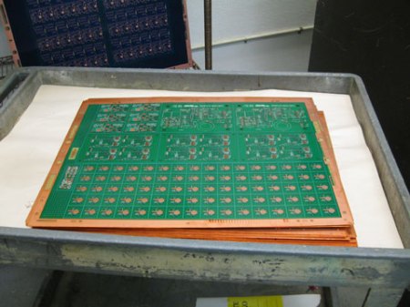
Although not a hack in itself, many of you may be interested in seeing how a printed circuit board is made in the manufacturing world.  This tour of Advanced Circuits does a good job of explaining the process. The article explains how a PCB will go through a CAD/CAM review, drilling, deburring, and the various chemical etch, plating, and curing processes.

Although many hackers make their own PCBs, having it professionally done can be a good option depending on how many copies are needed. One benefit of this is that PCBs can be checked by an optical inspection process, or even by a “flying lead” machine which works by contacting leads automatically in a computer controlled setup.

A video of this incredible machine is included after the break.  Around 0:26 is when it really starts to get going. Continue reading “Tour Of Advanced Circuits – A PCB Manufacturer”

Semi-automatic PCB Drill Press

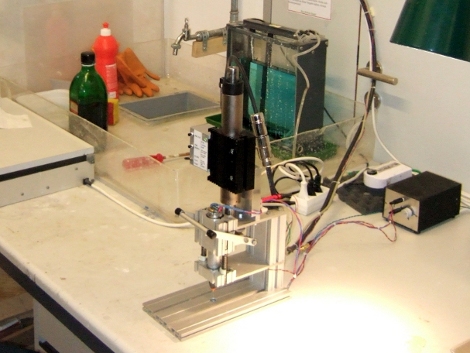
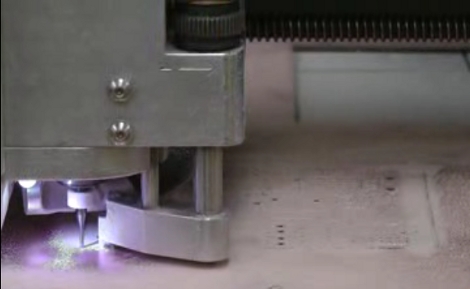
Kiss the days of breaking bits while drilling through-hole PCBs goodbye thanks to this semi-automatic drill press (translated). Now it’s not going to line up the bit with the exact location of the hole (that would make it a fully automatic drill press). This works by lining up the board manually, then stepping on a pedal to activate the plunging motion of the drill.

A linear motor is responsible for the smooth, accurate motion along the Z-axis. Many hobby setups use a Dremel drill press, or even rely on prayer-based systems such as doing it free-hand with a rotary tool or by using a piece of acrylic as a guide hole. The hobby drill press tends to have some play in it and free-handing with tiny bits that are as fragile as glass both result in far too many broken drill bits. In the video after the break you can see that the linear motion is perfectly plumb with the table of the device, preventing the movements that cause breakage. The addition of the pedal makes it easy to position the boards because you can use both hands.

Having a tool like this takes all of the frustration out of using through-hole parts.

Continue reading “Semi-automatic PCB Drill Press”

Snap-together PCB Mill

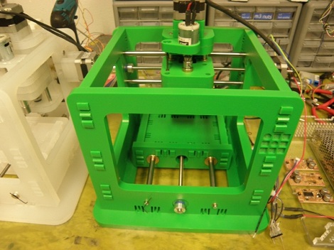
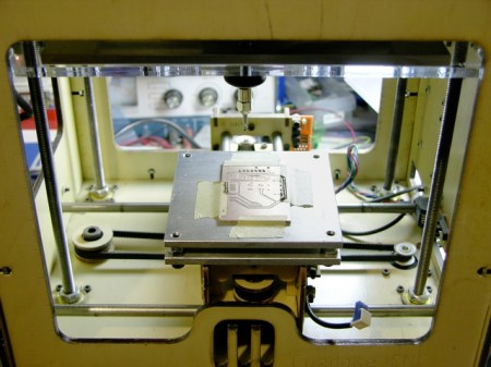
[Jonathan Ward] came up with the MTM Snap, a snap-together pcb mill as part of the Machines That Make group at MIT.

We covered [Jonathan]‘s previous work made out of half-inch plywood, but the new iteration of his PCB includes a clever snap-together mechanism instead of screws and bolts. Although the MTM Snap looks a lot like3d printers such as a reprap, the similarities end with the off-the-shelf stepper motors. Instead of using motor drivers and control electronics from a reprap, the project uses custom stepper drivers, controlled by a bare Arduino.

We’re really impressed with the results of the MTM Snap compared with what is possible on a reprap-derived milling machine like a makerbot or wolfstrap. We’re thinking that’s due to the mass of this project compared to the printed ABS parts of the ‘common’ 3d printers, but any MEs are more than happy to correct that notion.

Check out the video after the break to see the machine in action and a great view of the snap-fit mechanism.

Continue reading “Snap-together PCB Mill”

PCB Milling With A Makerbot

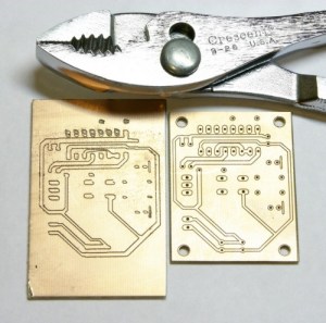
[Keith] wanted to use his makerbot for some PCB milling, but he ran into a pretty big problem. The platform that his PCB would sit on was mounted with a layer of double sided foam tape and was not perfectly aligned to the head. Not only that, but it would tilt when pressure was applied. This made the result of the milling completely unacceptable. To remedy this, he made a new platform that is not only rigid, but he has made it so that there is the ability to adjust it for perfect alignment via adjustment screws in the 4 corners. At the beginning of each session, he can be absolutely sure that everything is aligned perfectly and his PCBs show a huge improvement. You can see a comparison of the two in the following picture.

[via HackedGadgets]

PCB Milling Tutorial

[Juan Jose Chong] put together a set of videos and a PDF guide to milling printed circuit boards. You’ll find the pair of videos, totaling about twenty-two minutes, embedded after the break. In them, [Jaun] details the techniques used by the IEEE chapter at Texas Tech University to mill PCBs instead of using the traditional method of etching them. We’ve long been a fan of milled PCBs and often dream about the day we can retire the old iron we use for the toner transfer method.

In the tutorial, IsoPro is the software used to control the mill. The CAM files from a PCB design program are imported – they can come from many different programs including EagleCAD. A few setup steps let the operator configure the resolution necessary to mill the correct tolerance and from there the paths that outline each trace are calculated in software. In order to facilitate double-sided boards a reference hole is drilled in the copper clad board to accept a post on the mill table. Tape down the substrate with some foil tape, set the depth of the end mill bit, and let the machine do its thing. [Juan’s] video illustrates how quickly this can produce a rather complicated board, finishing in around 20 minutes.

Continue reading “PCB Milling Tutorial”

mobo_salvage

PCB Parts Salvaging Made Easy

Take a moment to think about how many old or damaged computer motherboards you have tossed away over the years. Sure we try to repurpose everything we can, but reclaiming electronic components from complex devices can be overly time consuming if you don’t have the proper means of doing so.

Ideally, if we were to try removing components from a motherboard, an old stove or an unused toaster oven would be great. If you didn’t have either item at your disposal, you could always attack the board with a soldering iron and some braid – but who has the time for that?

[Giorgos Lazaridis] over at PCBHeaven put together a quick video demonstrating his favorite technique for salvaging components after a motherboard has outlived its usefulness. Using a 2000W heat gun, a few hand tools, and couple of metal pans, he had the entire board stripped bare in about 30 minutes time. He talks about some of the best parts he has discovered while salvaging and points out a few hard-to-find items that can be easily obtained by tearing down a motherboard.

Sure his process might not be as easy as inverting a PCB in an oven, but his method is cheap, portable, and takes up very little space.

Keep reading to see [Giorgos’] video demonstration and don’t forget to check out some of the other cool stuff he has done in the past, such as his temperature-controlled soldering station, this acrylic bender, or this bench top function generator.

Continue reading “PCB Parts Salvaging Made Easy”

PCBs Without Any Substrate

[Kimio Kosaka] is taking the concept of free-formed circuits to the next level with O’Baka Project No.7. It’s a fully functioning Arduino board, without the board. The traces are there and provide all of the support for the rest of the hardware. You can imagine the fragility of the package so it won’t be a surprise to learn that O’Baka Project means ‘stupid’ project.

We don’t think this manufacturing process is completely worthless. The ‘board’ seen above looks quite interesting and might be a good idea when building a show-piece where you want the circuitry to be seen. [Kimio] describes the process he used to achieve this look. The first step is to design a single-sided circuit board; he used EagleCAD. After printing out the traces he used 0.46mm steel wire to trace out each connection. Now heat up that soldering iron – [Kimio] recommends using high-acid flux to ease the process of soldering to the steel.

We think this would nicely compliment projects like LED cubes that use the circuit itself as a support structure. See this Arduino alternative from several different angles in the video after the break.

Continue reading “PCBs Without Any Substrate”