We’ve reduced printed circuit board design to practice so much that we hardly give a thought to the details anymore. It’s so easy to bang out a design, send it to a fab house, and have ten boards in your hands in no time at all. All the design complexities are largely hidden from us, abstracted down to a few checkboxes on the vendor’s website.
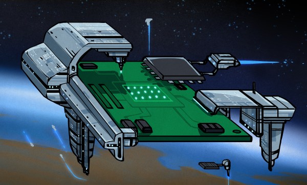
There’s no doubt that making professional PCB design tools available to the hobbyist has been a net benefit, but there a downside. Not every PCB design can be boiled down to the “one from column A, one from column B” approach. There are plenty of applications where stock materials and manufacturing techniques just won’t cut it. PCBs designed to operate in space is one such application, and while few of us will ever be lucky enough to have a widget blasted to infinity and beyond, learning what’s behind space-rated PCBs is pretty interesting.


