It’s a problem that few of us will ever face, but if you ever have to calibrate your scanning electron microscope, you’ll need a resolution target with a high contrast under an electron beam. This requires an extremely small pattern of alternating high and low-density materials, which [ProjectsInFlight] created in his latest video by depositing gold nanoparticles on a silicon slide.
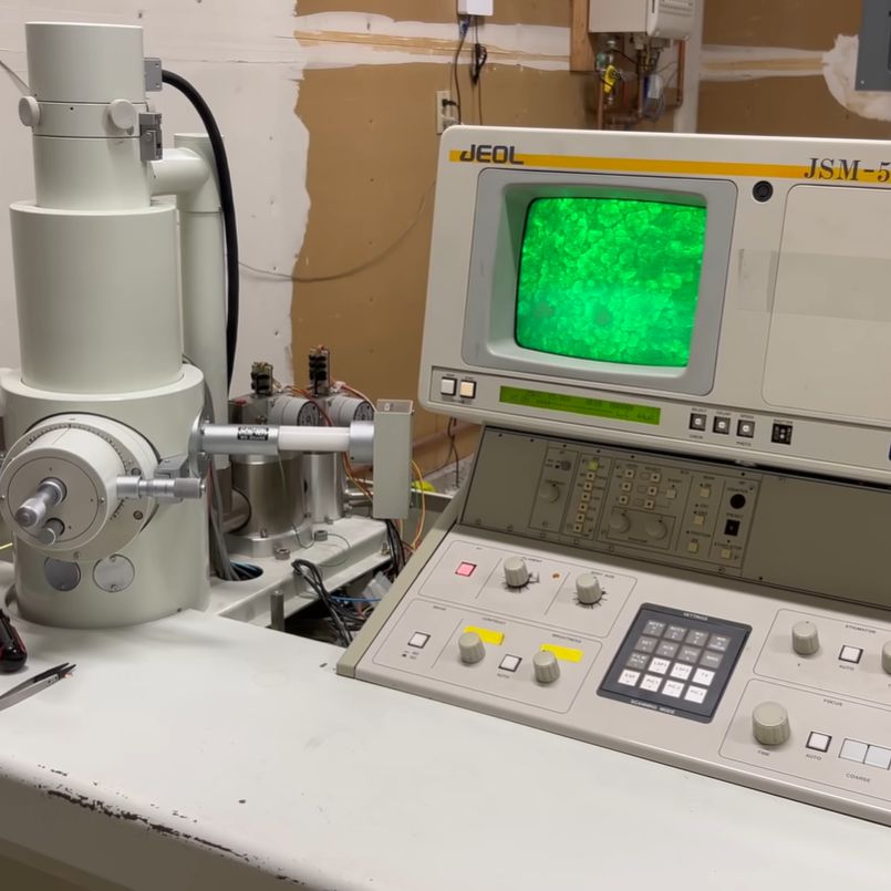
[ProjectsInFlight]’s scanning electron microscope came from a lab that discarded it as nonfunctional, and as we’ve seen before, he’s since been getting it back into working condition. When it was new, it could magnify 200,000 times and resolve features of 5.5 nm, and a resolution target with a range of feature sizes would indicate how high a magnification the microscope could still reach. [ProjectsInFlight] could also use the target to make before-and-after comparisons for his repairs, and to properly adjust the electron beam.
Since it’s easy to get very flat silicon wafers, [ProjectsInFlight] settled on these as the low-density portion of the target, and deposited a range of sizes of gold nanoparticles onto them as the high-density portion. To make the nanoparticles, he started by dissolving a small sample of gold in aqua regia to make chloroauric acid, then reduced this back to gold nanoparticles using sodium citrate. This gave particles in the 50-100 nanometer range, but [ProjectsInFlight] also needed some larger particles. This proved troublesome for a while, until he learned that he needed to cool the reaction temperature solution to near freezing before making the nanoparticles.
Using these particles, [ProjectsInFlight] was able to tune the astigmatism settings on the microscope’s electron beam so that it could clearly resolve the larger particles, and just barely see the smaller particles – quite an achievement considering that they’re under 100 nanometers across!
Electron microscopes are still a pretty rare build, but not unheard-of. If you ever find one that’s broken, it could be a worthwhile investment.
Continue reading “DIY Calibration Target For Electron Microscopes”