We’re no strangers to looking at uncapped silicon. This time around it’s not just a show and tell, as one transistor form a ULN2003 chip is reverse engineered.
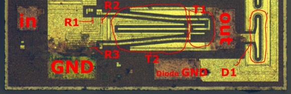
The photo above is just one slice from a picture of the chip after having its plastic housing remove (decapped). It might be a stretch to call this reverse engineering. It’s more of a tutorial on how to take a functional schematic and figure out how each component is placed on a photograph of a chip die. Datasheets usually include these schematics so that engineers know what to expect from the hardware. But knowing what a resistor or transistor looks like on the die is another story altogether.
The problem is that you can’t just look at a two dimensional image like the one above. These semiconducting elements are manufactured in three dimensions. The article illustrates where the N and P type materials are located on the transistor using a high-res photo and a reference diagram.
If you want to photograph your own chip dies there are a few ways to decap them at home.