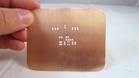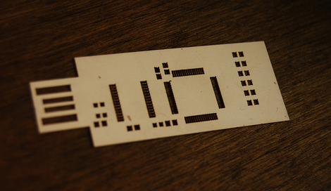
Even if you’ve overcome your fear diddling about with tiny SMD components, applying solder paste – especially if you’re populating more than one board at a time – is still a chore. The pros use very expensive laser cut stainless steel solder paste stencils, something still a bit out of reach to the casual hobbyist. [Felix] solved this problem by making his own solder paste stencils very cheaply using empty soda cans.
The process begins just like any other home etching tutorial by lightly sanding the un-bent aluminum can and applying the etch resist via the toner transfer method. Etching is done with off-the-shelf HCl and hydrogen peroxide, resulting in an amazingly clean stencil comparable in quality with a professional stencil.
Sure, going through a dozen-step process to make a solder paste stencil may not be as convienent as [Cnlohr]’s toothpick and tweezers method, but [Felix]’ method is just about up to par with extraordinarily expensive laser cut stainless steel stencils. Not bad for something that came from the recycling bin.


