For the last five months, I’ve been writing a series of posts describing how to build a PCB in every piece of software out there. Every post in this series takes a reference schematic and board, and recreates all the elements in a completely new PCB tool.
There are three reasons why this sort of review is valuable. First, each post in this series is effectively a review of a particular tool. Already we’ve done Fritzing (thumbs down), KiCad (thumbs up), Eagle (thumbs up), and Protel Autotrax (interesting from a historical perspective). Secondly, each post in this series is a quick getting started guide for each PCB tool. Since the reference schematic and board are sufficiently complex for 90% of common PCB design tasks, each of these posts is a quick how-to guide for a specific tool. Thirdly, this series of posts serves as a basis of comparison between different tools. For example, you can do anything you want in KiCad and most of what you want in Eagle. Fritzing is terrible, and Autotrax is the digital version of the rub-on traces you bought at Radio Shack in 1987.
With that introduction out of the way, let’s get cranking on Upverter.
A little bit about Upverter
Upverter was founded in 2010 as an entirely web-based EDA tool aimed at students, hobbyists, and Open Hardware circuit designers. This was one of the first completely web-based circuit design tools and Upverter’s relative success has been a bellwether for other completely web-based EDA tools such as circuits.io and EasyEDA.
I would like to take a second to mention Upverter is a Y Combinator company (W11), which virtually guarantees this post will make it to the top of Hacker News. Go fight for imaginary Internet points amongst yourselves.
Upverter is a business after all, so how are they making money? Most EDA suites offer a free, limited version for personal, hobbyist, and ‘maker’ projects, and Upverter is no exception. The professional tier offers a few more features including CAM export, 3D preview, an API, simulation (coming soon), BOM management, and unlimited private projects for $125 per seat per month, or $1200 per seat per year.
To give you a basis of comparison for that subscription fee, Eagle CAD’s new license scheme gives you everything – 999 schematic sheets, 16 layers, and unlimited board area – for $65 per month, or $500 per year. Altium’s CircuitStudio comes in at $1000 for a one-year license. There are more expensive EDA suites such as Altium Designer and OrCAD, but you have to call a sales guy just to get a price.
Upverter is positioning itself as a professional tool at a professional price. There are better tools out there, of course, but there are thousands of businesses out there designing products with tools that cost $500 to $1000 per seat per year. In any event, this is all academic; the Hackaday crowd gravitates towards the free end of the market, whether that means beer or speech.
A big draw for Upverter is their Parts Concierge service. You’ll never have to create a part from scratch again, so the sales copy says. Apparently, Upverter is using a combination of very slick scripts to pull part layouts off a datasheet and human intervention / sanity check to create these parts. Does it work? We’re going to find out in the review below.
Creating A Schematic
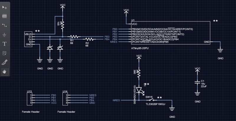
We have three things to do in Upverter. First, we’re going to recreate the schematic given in the introduction to this series of posts. Second, we’re going to make a part from scratch in Upverter. In this case, we’re going to build the PDIP ATtiny85. Finally, we’re going to turn this schematic into a board. Let’s begin with the end. Here’s the completed schematic:
This is, more or less, exactly what we want. Here’s how I got to this point.
Upverter’s main focus and selling point is that you never need to worry about part libraries. There are only so many footprints, there are only so many datasheets, and this is a web-based EDA tool, anyway; it only makes sense every part should be available. In practice, or at least for the jellybean parts I’m using for this simple microcontroller board, everything pretty much works out. A 1×4 0.1″ header is the same no matter who the manufacturer is.
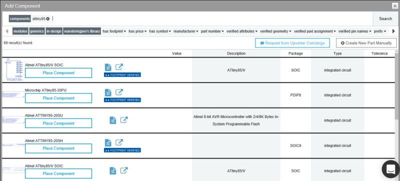
Clicking on the little chip icon in the toolbar brings up the Add Component dialog. Search for a part, use the search filters, and you’ll probably find what you’re looking for.
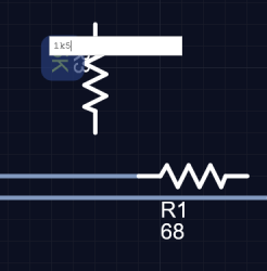
With the parts selected and laid out, the only thing left to do is draw a few wires, place a few VCC and GND symbols, and name all the nets. This is easy enough with the toolbar on the left-hand side of the screen. For those of us who aren’t quite into the whole Web 2.0 thing, Upverter provides hotkeys. Press ‘N’ to add a net, ‘F’ to flip a selection, ‘R’ to rotate a selection, and arrow keys to move the window around.
For anyone who has used PCB design software before, all of this should be familiar. There are a few oddities of the Upverter schematic interface, though:
- Resistors, caps, and everything else that comes in standard packages is easy. Everything else — inductors and switches — is hard to find in the interface.
- For some ungodly reason, Upverter thinks your mouse only has one button. Dragging the view around with the ‘hand’ tool is a chore.
- Values can be edited directly on the schematic, not just through the modal dialog accessed by double clicking a part.
- The bus icon is a ‘wheels on the bus’ bus.
Making A Part From Scratch
Upverter has a lot of parts in their database, and they have a Part Concierge service that will make parts for you. For this part of this tutorial and review, we don’t care about that. This is how you create a PDIP ATtiny85 from scratch. Does Upverter already have a PDIP ATtiny85 part? Yes, but that’s not the point of why I’m doing this.
There’s a reasonably complete and up to date guide on the Upverter wiki, although there are a few tweaks and caveats that should be mentioned and are not obvious at all.
The first thing to do when creating a part from scratch in Upverter is to edit the attributes of the part. These attributes include the part number, manufacturer, package, a link to a datasheet, Digikey and Mouser part numbers, and temperature ratings. This is a simple chip for a simple board that will only be used once, so entering ‘ATtiny85’ in the name field is good enough.
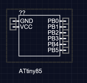
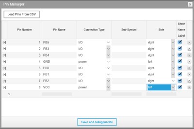
Next up is generating pins for the schematic symbol. Click on the ‘Pins’ label in the right hand toolbar, click the ‘edit’ button, and the Pin Manager dialog pops up. The first column is the pin number, in this case starting at one, going counter clockwise around a PDIP part. Refer to the ATtiny85 datasheet for the second column, the pin name. That’s PB0 through PB5, VCC, and GND. The next few columns define the function of the pin, and which side of the schematic symbol they’ll be autogenerated on. Hit ‘save’ in the Pin Manager, and you’ll have something like the picture on the right. That’s not bad, actually.
With the schematic symbol out of the way, it’s time to make the footprint.
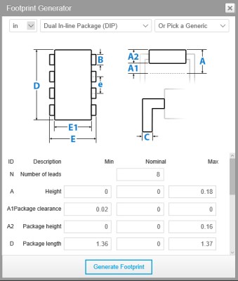
At the top menu bar, hit the Footprint button, and click the footprint icon on the left-hand toolbar. This gets really cool.
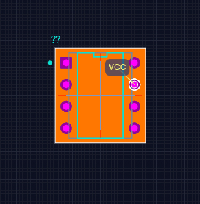
The Footprint Generator has options for just about every type of package you’ll ever need. If you need a DIP, select DIP from the drop-down menu. If you’re working with an SSOP part, select that. Selecting any standard brings up options for the number of leads, the height of the package, the pitch of the leads, and all the dimensions you’d find in the back pages of a datasheet. I couldn’t find any options for truly weird and old parts like PGA packages, but Upverter’s footprint generator is more than enough to automagically create parts by just entering numbers from a datasheet. It’s pretty cool.
With the schematic and a custom part done, it’s time to move on to the last step: actually creating a PCB.
Creating A PCB
We’re done with the schematic, so hit the ‘PCB Layout’ button at the top of the screen. Here’s what we get:
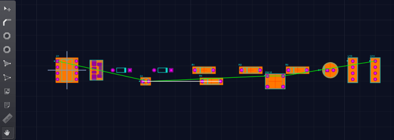
It looks ugly, but that’s fine double click on the background of the window to open the Board Outline dialog. This is where you set the dimensions of the board. Since we’re just copying the board presented in the introduction to this series of posts, enter 44.45mm x 20.95mm in the dialog. Move the components around, and you’ll eventually get something that looks like this:
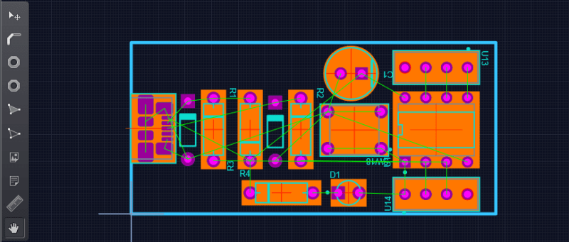
 Again, we’re simply copying what we’ve already done half a dozen times now. Routing is easy enough with snap-to and a neat feature I’ve only seen in Photoshop, Illustrator, and their ilk — automatic alignment to other pads.
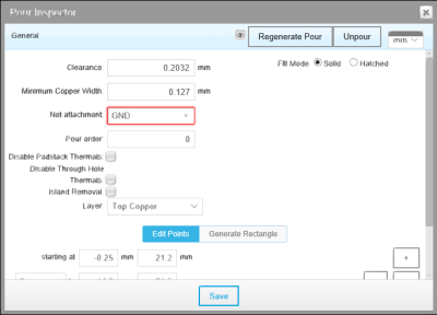
The only confusing part about this build is the ground and power pours. Here’s the trick: to stop drawing a pour polygon, press escape.
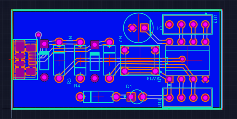
Draw a pour on the top copper layer, assign it to the GND net, draw a pour on the bottom copper layer, assign it to the VCC net, and get the VCC pad on the USB connector to the other side. That’s it, it’s done:
Sending the board off, exporting, and the takeaway
Want to take a look at this project for yourself? That’s one of the bonuses of a web-based tool. Here you go.
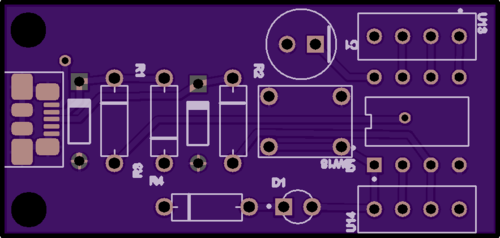
Upverter allows you to design a PCB in their tool, but strangely they don’t have an agreement with anyone to sell the actual small production runs. I find this very odd; it’s a great way to make a bit of change for Upverter. Fritzing, for instance, has an agreement with a fab house in Berlin to produce boards at about a 300% markup over OSH Park.
Instead of upselling, Upverter has a spectacular array of options to export a bunch of data. Everything from pick and place data to 3D models in STEP format is available. Gerbers are just a single download button away, and yes, they work with OSH Park’s web interface.
Final Thoughts
So, how does Upverter compare to other design tools? Remarkably well, in my opinion. It’s much more refined than the more primitive tools I’ve taken a look at. Routing is easy, and even building a part from scratch is relatively simple. Is it good enough for a hobbyist? Absolutely. Is it good enough for a team of engineers? That’s another question entirely.
When it comes to EDA tools that cost money, there are two tiers. Altium and OrCAD are the top tier. You can’t even get a price for these things without calling a salesperson. The second tier includes Eagle CAD, which is significantly cheaper than a yearly subscription to Upverter. Again, the Hackaday crowd gravitates towards free as in beer and speech, but it is something to think about.
One problem I did have with Upverter was a few graphical glitches. To be fair, I was running this in Microsoft Edge, but a few times in creating this tutorial Upverter turned into the cover of a vaporwave album. Whether this is Upverter or Edge is up in the air, but it is an issue.
Well that’s done
This concludes the Creating A PCB in Everything post on Upverter. If you have a suggestion for what PCB design tool to cover next, leave a note in the comments.






I tried upverter a couple of years ago (when it was pretty new, not sure how much has changed) but I found it to be somewhat slow at redrawing the board layout when panning. I found this too frustrating to continue with. Around that time CircuitMaker from altium was released. I would sincerely recommend it. Free and capable. Honestly for the typical ‘hacker’ it is hard to make an argument that paying for EDA at the moment is worth it, KiCad seems to be on the way up and CircuitMaker is already there in my mind. Give it a go! Over and out.
you should do Cadence Allegro, Mentor DxDesigner, and Zuken if you really want to spend some $ ;-)
Yeah, I doubt I’ll be doing another one of these. The ratio of time required to do and write these things is not consummate with 1) the views we get on these posts, and 2) the number of times it’s shared on social media.
Basically, it’s not worth spending time on this crap.
This post was a hail mary; Upverter is a Y Combinator company which guarantees this post will hit a top slot on Hacker News, provided someone submits it. Then, hopefully, someone will notice I’ve written a book-length series on making PCBs in different software tools and submit those posts. That would make continuing this series worth it.
It’s the usual song and dance: Hackaday readers say they would like to consume some content, but don’t actually follow through when we produce that content.
I guess I’ll go write some perfect troll bait. That’s the most commented post in Hackaday history, right there. If you think media sucks, you have no one to blame other than yourself.
>If you think media sucks, you have no one to blame other than yourself.
What about the system by which writers are paid for having lots of people read an article, rather than for creating high-quality articles? Also, the people who comment on good articles like these might not be the same ones who comment on clickbait like you linked to, so the ones you’re complaining to here might not actually be the ones at fault (Ctrl+F “Clay” on that article turns up nothing, so I’m allowed to say that).
> What about the system by which writers are paid for having lots of people read an article, rather than for creating high-quality articles?
I get paid the same either way, but shitting onto a keyboard is faster.
Sure, but that just makes you a run of the mill shitter ;-)
Writing about niche, specialized, high value, hard to get into particular field, high level stuff attracts special kind of people. Not the click on a clickbait fb cattle, but actual industry professionals, influencers and people with money to spend.
Its the question of what kind of crowd do you want to attract, the choice between h3whatever piedewpie YT drama 14yr old meme lords from 4chan versus people willing to actually read 4 pages of text about something highly technical, the crowd worth $$ to advertisers. There is a reason highly specialized industrial keywords/clicks are multiple times more lucrative than average ad impression served on a 50mil views YT badly animated birthday song watched by 6 year olds on mums phone in a loop, or lego unboxing vids.
Some people go first route and devolve like hmm Linustechtips? ign.com?
Fun fact: The most perfect, highest-quality product in the history of mankind was produced with years of care and dedication and completed in 1762. Nobody knows what it was because the creator starved to death.
Turns out you can’t live on craftsmanship, and nobody will buy the most perfect product unless it’s a product they want.
2) the number of times it’s shared on social media.
I like Facebook and Twitter as much as I like stomach flu.. Even if I did post of Facebook, posting a HaD link would be unlikely since virtually none of my friends or family are HaD readers.
Hey Benchoff, slow your roll man. I’ve actually read the whole series and came back to the Kicad one a few times now since I’m trying to learn that turkey after using Eagle and then Diptrace. I’m now working on a Pi Hat using Kicad, and I doubt I’d have bothered trying it otherwise. Muchas gracias, amigo.
Yeah, rest assured we do read it, if only to confirm the dead bug technique is a good idea.
I have to +1 this one as well. Because of your KiCad article, I decided to learn KiCad and use it for my next project. It turns out, I really like it, and it was quite well timed, given the changes in the Eagle licenses.
You’re doing good; it’s just apparently not with the social sharing crowd.
Agree with Dielectric. I was using ExpressPCB forever, then found Eagle to rung PCB-2-GCode on my router and found out KiCAD can do the same, since it exports Gerbers. Slow your roll, Benchoff, You write a great article, don’t reduce it with pooping on the keyboard comments.
Well… the bulk of the readers of H-a-D already mostly use a PCB package, they already have made their choice, if your goal of writing these series was to generate clicks, well that’s not a well founded plan, they are not going to be too interested in other products than the one they use, and they are not going to like it when you make errors in the evaluation or bitch about the product they do use.
If your goal was to help people who want to choose, or re-choose, a PCB package then you probably didn’t pick good choices, or focused too much.
3 articles on Eagle. 3 articles on KiCAD – did you really need 3 articles about such packages, you can’t cover everything in the packages in 10 times that many articles, so by necessity you are giving an overview, that could be done in 1 article each, with a couple sections “what I like”, “what I don’t”.
An article on Autotrax. Seriously. What’s the point. Why would you put any effort into an article about that, it can only be a historical curiosity, it’s not helping somebody make a decision, nobody is going to say “oh boy, autotrax looks sweeeeet I’ll be using that for sure!”
Your article on Fritzing has various errors and biases, but actually wasn’t far from the general overview that is useful.
This article on Upverter probably is best in actually what the articles should be, the quick overview highlighting the main points.
However both Fritzing and Upverter are bit-players, only slightly more relevant for decision making than Autotrax. Most H-a-D readers are going to be interested in choosing between the big players, Eagle, KiCAD, DipTrace, and the Altium offerings.
On the contrary, I think that this has been some of the best content I’ve read on Hackaday, and it’s actually the reason why I continuously check Hackaday. I was waiting for you to cover DipTrace, and perhaps a couple others, leading to an epic royal rumble between the PCB CAD programs. I’m sure I’m not the only one who would share this until it attains the popularity it deserves.
It reminds me of techreport’s well regarded series, SSD endurance experiment – in length and substance. It would also help out a lot of new players, as most of my friends in uni default to Fritzing, which, while it has it’s uses, gave me a headache in actual use trying to layout a board.
I really hope this series can be continued!
Brian: it’s clear to me you are a good writer. Making technology sound not just interesting but funn/funny is a challenge. Your posts always make at least one attempt at good humor. Sometimes you nail it. Sometimes it falls flat. Sometimes it reads a little snarky. But I realize this is the nature of formal writing. We can’t all be Shakespeare.
At any rate I respect what you are doing (published writer myself. I know it’s hard).
I think this particular series has a lot of value for people LOOKS ng for their first PCB tool. And any competent engineer should always at least be AWARE of other tools available, even if they never plan to switch.
But your comments in articles often leaves me felling like you don’t want to be here.
It was enough to explain your strategy of trying to get clicks via the Ycombi link. That would have sufficed.
Yet you went the additional step of insulting your readership.
You have done that regularly.
If you do not like tthemindset of the HAD readership, or can’t take their criticisms, or dislike their last attitude about promoting Had or posting comments, you really only have two options:
1: work to ENCOURAGE the behavior you want, gently discourage that which you don’t, and learn when to just leave some shit alone.
2: find a new job.
I hope it goes without saying that I hope you choose the first option ;)
At the risk of encouraging the behavior by replying (“engagement”) to Brian’s troll thread, this. The PCB In Everything series is one of the best, and most useful, things I’ve seen on HaD in the last year (or more). Even my day-job EE dept. is referencing this series in having the heart-wrenching discussion of whether to stay with EAGLE or not following the change to subscription model. Kudos on a job well done!
That said, the active contempt shown for the reader in some of Brian’s posts and followup comments is a real turn-off. If you’re just looking for mountains of low-quality engagement (and to be butthurt if you don’t get it), a well-researched quality series on a niche topic like PCB design software won’t get it. This series has surely cultivated the kind of audience and engagement that call-for-quote PCB software companies will pay dollars-a-click for and maybe $hundreds if it leads to a sale… but it’s not the kind of thing people share with Grandma on facebook. If count-of-clicks is all that matters, one can definitely take the easy way out and drop a vi-vs-emacs article or thinly-veiled political rant to generate large argument threads. Orville Redenbacher will happily snap up that ad space at .02 cents a click, but it will have the high-value advertisers fleeing and probably doesn’t look good on a resume.
I don’t get it. I’ve read every article, I think, and keep a few open as reference on either of my computers. Are you judging the value of the articles based only on number of comments? Because if that is the case, you’ll drown in clickbait articles that just taunt the trolls into responding. But if that’s the way you want to see HAD go . . .
I actually enjoyed these series, I think it is very well written and informative. I learned Schematic/PCB using PCAD back in the late 90s. At work we use Altium Designer, but I am always looking for something better. I look forward for your series. I gave kicad a try because of it.
For my hobby stuff I use upverter and I like it. I like how I can start something at work, work on it from home or if I am out on the road without having to worry about library sync issues or revisions mismatch. I made my entry to the 1kb challenge using that took me less than 2 hours from beginning to end. The zip file you get from the export can be uploaded direct to OSHPpark without having to deal with renaming, etc.
I’ve gotten pretty passionate about Altium since I started using it 2 years ago. Suppose I could do a write-up and submit it via the tip line?
Decal wizards are nice and all, but I would love to see how the Parts Concierge would handle much more complicated footprints, like ones from integrated DC/DC converters. It’s easy to say “there’s only so many footprints” and then you get something like this.
Oh sweet Jesus that package is ridiculous. I saw the photo of it and laughed, then I scrolled down and saw “*Patent pending package” and laughed harder. Why would you bother patenting a package that nobody would want to copy anyway?
If it’s ridiculous but it works, it’s not ridiculous.
Maxim 43 If it’s stupid and it works, it’s still stupid and you’re lucky. Fits design as well as anything.
But it’s not stupid, just ridiculous. And I don’t think luck had anything to do with it.
To be fair, heavier-than-air fixed wing craft was an obviously stupid idea at the time.
Space concerns are *huge* for DC/DC converters – anything you can do to shrink the size of a solution will instantly get people banging on your door. The super-odd packages are usually the result of a multi-module solution, where you literally place the die of the control chip in one location, FETs in another, an actual inductor in another, etc. Then you overmold the whole thing and poof, there’s your converter chip.
So yeah, it looks nuts, but it can save a ton of space compared to a controller + FETs + inductor, all of which would need their own package/lands on the board. Note that the *package* that’s being patented isn’t the land pattern – you can’t patent a land pattern.
Honestly, the worst thing about that package is the way they documented it.
…
You assume a lot that isn’t evident. Package design is a serious amount of work and gaining any advantage over other manufacturers is better. Why is the package ridiculous BTW? To me it looks to be carefully designed for its purpose – integrating a DC/DC converter in a compact package while eliminating unnecessary signal routing. That includes thermal design which I assume is what is patented – given (as posted by Pat´below) land patterns aren’t patentable.
And I thought I’d never see one of these devices again!!!!
They are terrible in layout and they are unreliable:
The mainboard I dealt with had these (ok similar part by intersil) as part of its VRM circuit.
One had shorted high but they wouldn’t force a low to save the CPU and kick the PSU short-circuit protection in.
Also they didn’t start up keeping the low-side on as a hardware protection.
Only the CPU had fried. Removed the chip, read multiple datasheets to work out how to disable the missing phase for the controller (externally configurable for multiple model PCBs via a resistor/jumper system).
Replaced the CPU, checked for safety margin(basic math) and got my qualified team-leader to approve.
Easy using Kicad.
I don’t mean to criticize, but unless KiCad literally does the footprint for you (which is what the Part Concierge thing is supposed to be), you can’t possibly say “Easy” for that part. Is it doable? Sure, but it’s not easy, because just trying to read the datasheet and decode what the dimensions are on that part is hard enough, and that has nothing to do with the software. *Especially* when you add in the stencil layer.
It apparently actually seems to work on mobile, though you probably want to use a stylus. Cool. :)
“For some ungodly reason, Upverter thinks your mouse only has one button.”
because dumbass hipster apple bastards think every mouse should only have one button cause “users would get confused with more than one button”
*dons flame suit*
I wonder if it supports trackpad gestures for pan, zoom, etc? Because all of the best engineering gets done on a Macbook at the coffee place around the corner.
All hail the trackball!
I wasn’t aware Apple made a magic trackball.
That was Apple of old where a discoverable hardware button attached to a device that already have another button was to hard to grasp – the new Apple instead makes devices where there are no UI buttons at all but one is expected to know how to gesture on a flat surface instead. But that isn’t the worst, now they even make devices where the level of force used for the gestures can have effects on the UI.
I’m just getting into CAD for PCB’s which one should I choose? I want one that will be acceptable to use in industry but I don’t want subscription or high prices (not asking much eh?), I think I was heading for Eagle but now I am not too sure because of their pricing model. If anyone has any non fanboy advice I would love to hear it. I am open to the likes of Kicad but how well does this compare to low end commercial software? I don’t want software that is nearly there I want something that works and isn’t just going to stop being useful in say 5 years time.
Any help greatly appreciated.
Literally nobody in industry uses Eagle. Altium or Allegro.
KiCad has been fine for my personal projects.
They each do things a little differently though, so you might want to try a very simple circuit & layout in a couple of programs and pick the one you prefer.
I’m looking forward to some coverage of the gEDA family of tools, which include gEDA PCB/pcb-rnd, gschem, gerbv, icarus, and more.
http://geda-project.org/
http://wiki.geda-project.org/
There are also symbol, and footprint repositories, includng
http://www.gedasymbols.org/
as well the ability to use parametric footprint creation in the gEDA PCB fork, pcb-rnd
http://repo.hu/projects/pcb-rnd/
A lot of KiCad users rely on gerbv as their primary gerber review, and KiCad users also benefit from gEDA PCB footprints, which can be imported easily.
Tools like https://github.com/erichVK5/translate2geda also make even more formats of symbol and footprint available to gEDA users (Including Eagle, IBIS, BSDL, KiCad, gerber, and BXL, among others), and by extension, KiCad users. The PCB fork pcb-rnd can even load and save KiCad layouts.
The gschem schematic editor allows export of netlists to a variety of formats, not just gEDA PCB, including simulation software and other layout editors, both free and commercial.
In all, the gEDA project nicely augments the FOSS EDA ecosystem, and increases the pool of shared symbols, footprints and layouts available to hardware hackers.
“Upverter’s main focus and selling point is that you never need to worry about part libraries. There are only so many footprints, there are only so many datasheets, and this is a web-based EDA tool, anyway; it only makes sense every part should be available.”
This sounds like crap frankly. I’m pretty skeptical. I want low-level control over all the land patterns and schematic symbols, and if that’s not provided and you just “get what you’re given” that’s a dealbreaker for any professional use of the software, and it’s far worse than any paid software-as-a-service subscription controversy or anything like that.
Even for something like an 0603 package, careful tuning of the land pattern and solder paste pattern minimizes assembly problems such as tombstones. Not everything is just limited to something basic like a SOIC package or an 0805 resistor etc.
“Somebody on the Internet has provided a library for X part” is almost never trustworthy, and just like included other libraries with software tools, I find that everything requires my own library of custom parts that I’ve drawn from scratch, checked against the datasheet, and checked in proven assembly of the hardware. At the very least even a “good” library from somebody else almost always needs tuned a little bit and cleaned up. It’s just easier to check it yourself and re-draw it yourself in the process of checking it, so you know you’re not taking the risk.
How does the “part concierge” thing work? Are they actually paying people to sit there all day and draw libraries in response to customer requests?
Correctly drawing the schematic symbol in a sensible way for some given IC will make a schematic that is much cleaner and easier to read, compared to a “one size fits all” rectangular box with some pins.
They supply library information for every possible part and every possible package? Yeah right.
Here are five random examples chosen from my desk of real-world parts. I’d like the following:
How many of just these five examples are covered in the “never need to worry” Upverter libraries?
Vishay SiS427EDN in the PowerPak 1212 package.
Mini-Circuits MAC-85+
Generic zener diode in plastic SOD-323
Molex Ultra-Fit 3.50mm 1723101102
Bourns SRN8040 series power inductors.
The section about the parts concierge sounds a lot like InstaPart (on SnapEDA). Not sure whether they can export to Upverter or not, but they do export to Eagle, KiCad, Altium…
I don’t see Circuit Maker mentioned here, is there a reason for that? I just started using it without having used any software before and i think it’s great if you can cope that your design will be freely shared.
Hi Brain,
Thank you for your sharing. This series of articles are very helpful and well written.
You mentioined EasyEDA in this post and I hope you can cover EasyEDA in your next post.
EasyEDA is a cloud-based EDA tool suite which supports open source and working collaboratively, provides not only free PCB design(https://easyeda.com/editor), but also circuit design, Ngspice based simulation and RS-274X (Gerber) and Excellon gerber viewer, all are free.
They are also able to supply high quality PCBs at very low cost. It’s nice that users can download Gerbers and are not tied to the tool for PCB manufacture but they can buy PCBs and fully assembled PCBAs from EasyEDA if they wish.
It would be very cool to take a look at this one too. An actual step by step tutorial would be very helpful.
Thank you.
If they ain’t FOSS, available to install on my own server, then there’s something they are going to get:
– my freedom, my soul or sth. I don’t have idea about, but they for sure do !
Upverter really has the potential to be a fantastic EDA package. they have nailed some of the basic UI down in ways that could make it one of the most usable designers out there, at least for simple projects. the problem is that there is absolutely NO support, NO focus on fixing fundamental breaking bugs — take a look at their forum, there are bug reports on there going back several YEARS that are STILL not fixed. the company is so focused on its cash-cow (the concierge), and checkbox marketing features (3d preview, wh000p!?), that it has almost completely halted development on the designer itself. it’s a real shame, because features like collaborative editing, the package editor, the (quite extensive) part library and others combine to make a really compelling product – if it wasn’t for all the damn bugs. zac, if you’re reading this, get a freking QA team and fix the bugs already.
You should try EasyEDA (easyeda.com). It is a web-based EDA software.