By and large, automakers have spent much of the last century trying to make cars quieter and more comfortable. Noise from vehicles can be disruptive and just generally annoying, so it makes sense to minimise it where possible.
However, the noise from the average motor vehicle can serve a useful purpose. A running engine acts as an auditory warning to those nearby. This is particularly useful to help people avoid walking in front of moving vehicles, and is especially important for the visually impaired.
Electric vehicles, with their near-silent powertrains, have put this in jeopardy. Thus, from July 1st, 2019, the European Union will enforce regulations on the installation of noise-making devices on new electric and hybrid vehicles. They are referred to as the “Acoustic Vehicle Alert System”, and it’s been a hot area of development for some time now. Continue reading “Electric Cars Sound Off, Starting July 1st”→
In the hacker and DIY community, there are people who have exceptional knowledge and fantastic tools. These people are able to do what others could only dream about, and that others can only browse eBay looking for that one tool they need to do the job. One of these such people is [John McMaster]. He is the resident expert on looking inside integrated circuits. He drops acid on a chip, and he can tell you exactly how it works on the inside.
At the hardwear.io conference, [John] shared one of his techniques for reverse-engineering intgrated circuits. He’s doing this by simply looking at the transistors, and looking at the light they give off. He’s also looking at the wrong side of the die.
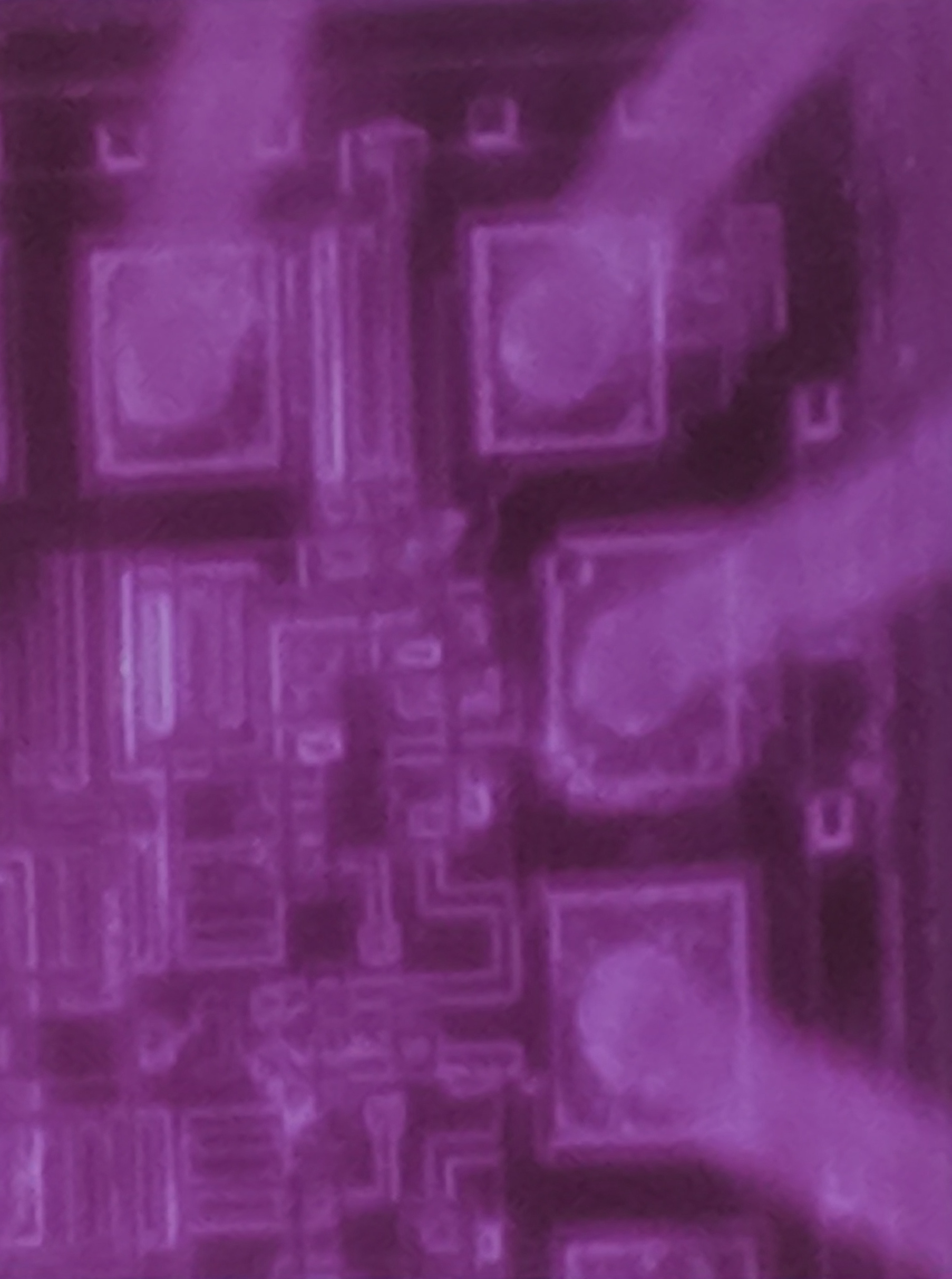
The technique [John] is using is properly called backside analysis, or looking at the infrared emissions of electron recombinations. This happens at the junction of every transistor when it’s active, and these photons are emitted at the bandgap of silicon, or about 1088 nm, far into the infrared. This sort of thing has been done before by [nedos] at CCC in 2013, but rarely have we seen a deep dive into the tools and techniques needed to look at the reverse side of an IC and see the photons coming off.
An IC, seen in infrared
There are several tools [John] used for this work, and he actually did a good comparison of different camera technologies used to image infrared photon emissions from integrated circuits. InGaAs cameras are expensive, but they offer high sensitivity. New back-illuminated CMOS cameras and cooled CCDs normally reserved for astrophotography were also tested, and as always, you get what you pay for; the most expensive cameras worked best, but there were ways you could make the cheap ones work.
As with any camera work, preparing the lighting is of utmost importance. This includes an IR pass filter, and using only LED lighting in the lab with no sunlight, incandescent, or halogen light bulbs in the room — you don’t want any IR, after all. A NIR objective in the microscope was sourced from eBay, for about 1/10th the normal cost, because the objective had a small, insignificant scratch. Using this NIR objective made the image twice as bright as any other method. You can successfully image a chip with this, and [John] tested the setup on a resistor inside a CD4050 chip; the resistor glowed a slight purple, the color you would expect with infrared sensors. But can it work with I/O levels in a more modern chip? Also, yes. It needs some Photoshop to process, and stretching the 12-bit or 16-bit color space into an 8-bit color space, but it does work.
Finally, the supreme achievement of doing backside IR analysis. Is that possible with even this minimal setup? This requires some preparation; the silicon substrate in an IC is transparent in IR, but there is attenuation and this is especially important when the substrate is 300 um thick. This needs to be shaved down to about 25 um thick, which surprisingly is best done with fine sandpaper and a finger.
While few IR emissions were observed via backside emissions, the original plan wasn’t to completely analyze the chip, but merely to do some floor planning. For this, it worked. It’s a remarkable amount of work to see the inside of a silicon chip.
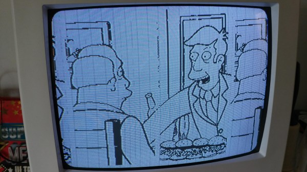
Maybe you’ve heard of a TV show called The Simpsons. Steamed Hams make a one-gag appearance in an unforgettable luncheon where Principal Skinner poker-faces his way out of a disaster with Superintendent Chalmers. Meanwhile, over on imgur, [Agumander] has put a black and white screencap from Steamed Hams in a printed circuit board.
The memory for this chip is an AT28C64, a 64 kilobit or 8 kilobyte steamed RAM. You call it a steamed RAM despite the fact that it is obviously a ROM. There is no microcontroller on this board or really anything resembling programmable logic. Everything is just logic chips. This board displays a 256×256 1 bit per pixel image over composite video. The sync is generated with the help of a 14MHz crystal and some circuitry taken from the original PONG board. Other than that, it’s just a bunch of NANDs and ORs that roll through the address space of the ROM and spit values out over a composite video port.
The build began by breadboarding everything save for a nifty solderless breadboard power adapter. Three ROM chips were programmed with different images — a cat, something to do with vaporwave, and some guy that looks like the poster from Eraserhead. Everything worked on the breadboard — yes, even at 14 MHz — so the build moved on to a printed circuit board.
The result is fantastic, and should work well on anything with a composite video port. We’re awarding bonus points for putting a socket on the ROM, simply so [Agumander] can change the image without whipping out the desoldering braid. If you need a refresher on Steamed Hams, it’s from the 7th season Simpsons episode ’22 Short Films About Springfield’.