Every so often, a new technology comes along that offers a broad range of benefits over what we already have. Just as lithium-ion batteries have made nickel-cadmium cells boring and old hat, gallium nitride semiconductors are making silicon parts look unimpressive by comparison. [Brian Dipert] looked at what this means in a practical sense by tearing down a GaN phone charger.
The charger in question is a 30 watt USB-C charger produced by Voltme. It cost [Brian] just $10, as prices of GaN hardware have come down significantly as economies of scale have kicked in. The charger measures just 1.2×1.3×1.2 inches, and weighs only 1.5 ounces. That compact size is thanks to GaN semiconductors, which are able to run cooler at higher power levels than their silicon forebearers.
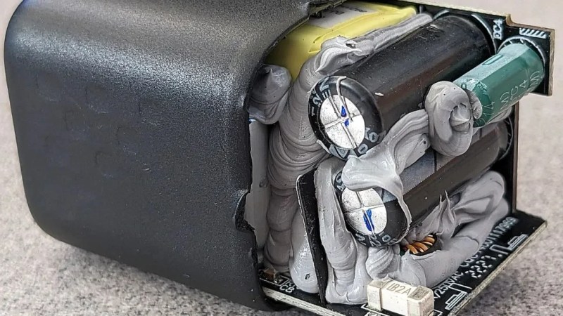
Cracking into the charger required levering open the case. The back panel came off with some work, revealing the mains terminals, which deliver AC power to the PCB inside via the case holding them in contact. Interestingly, the entire circuit inside is filled with an adhesive thermal goop, which helps pass heat from the hottest components to the charger’s case. [Brian] is able to guide us through the circuit, and he identified many of the major components. However, some of the markings on chips were beyond his research skills, and he asks any knowing readers to contribute their own information.
It’s interesting to see just what makes the high-powered compact chargers of today tick. Plus, it’s a hallmark of progress that what was once considered a wonder material can now be had in a $10 commodity phone charger from Amazon. How times change!


From a design standpoint are GaN MOSFETs any different from “normal” MOSFETs? Except the lower Rds ofcourse
450 mOhm Rds(on) doesn’t sound that impressive…
Even for MOSFETs running at line voltage?
These systems are always a balance of conduction loss (Rdson x Current) and switching loss (and cost). The lowest Rdson GaN transistor is 15mOhm (TP65H015G5WS) it can handle 100A continuous and output power of 10KW, but it would be a waste to use in a 30W USB adapter and would actually be less efficient due to the higher switching loss of such a large device.
GaN isn’t all that much magic in itself to be fair. There is plenty of non-GaN transistors on the market that would be just as good.
However. a GaN transistor likely uses less chip area for the same Rds-on. So it can likely be made cheaper now that GaN substrates aren’t as special anymore. (lithography costs is still a fair bit of production costs, so more chips/exposure = cheaper chips, as long as the difference in substrate costs aren’t too major that is.)
The whole point of GaN devices is that they do what non-GaN transistors cannot. Silicon technology is amazing in many ways but you can’t find a silicon power transistor with the same Qg, Ron, Vbr, and Eout. You might find a silicon part that matches or exceeds in one parameter, but not all simultaneously. You simply can’t achieve such high switching speeds in silicon parts at line voltage with the same efficiency.
If power supply designers could achieve in silicon what they can in GaN they would stay with silicon.
I thought the limiting factor of traditional MOSFETS was the current limitations caused by heat and that Gallium allowed more current to flow at those same temps.
As far as I’ve understood, GaN wins in Rds/input capacitance. Which means you can go: Faster and Smaller with Rds constant, or much lower Rds with input capacitance held constant.
The main advantage of GaN over Si MOSFETs is higher efficiency and smaller system size. A lot of the advantages of GaN power transistor is faster switching speed. (The time it takes to transition from on to off). This means lower loss during switching and therefore higher efficiency. Higher efficiency means less heat generated and less heat sinking is required. Lower switching loss also means you can operate at higher frequency without losing efficiency, and higher frequency operation means you can shrink the physical size of the passive components so the system is more compact.
GaN has a much higher figure of merit then Silicon. Meaning that you can have more power density, higher frequency, higher efficiency, longer lifespan or pick and trade between these things. GaN can allso operste at much hugher temperstures and so you dont need to cool it as much. Drawbacks of GaN are that it is more expensive and the smallest acheived transistor size is orders of magnitude larger then it is for silicon (not good for things like memory etc.).
In a power supply for example one way you can go with GaN is to make the switching power supply frequency higher this allows the power supply inductor which is a large and lossy component to be smaller.
Another way you can go is that the power supply can be more efficient and the GaN device can be hotter at the same time. This allows for the heat sink to be much smaller and so the supply can fit into smaller packages.
Regarding design with GaN. Things like small chargers are likely highly integrated and designed primarily by the fabricator of the GaN device so that the charger manufacturer is primarily just following or copying what it says to do on the data sheet.
The more detailed aspects of the design are however much different for GaN than for Silicon. GaN devices are depletion mode which means that they are on when the input voltage is 0V. They are off when the input voltage is negative. As a result more careful design is required in order to prevent catastrophic failures.
People who don’t know that Q is used to label transistors and that a four pin thingy with pin markings + – ~ ~ inside a power supply is most likely a rectifier, shouldn’t be allowed to post tear downs on edn.com.
Anyway, how much space did GaN save inside this device? Adding a D2PAK MOSFET doesn’t really add that much volume.
The space savings isn’t the MOSFET as much as the cooling. 30W of non-GaN power MOSFETs packed into that space would’ve been a fire and burn hazard.
GaN is a very different technology to silicon. The device package size is a very minor issue compared with significantly faster switching, body-diode reverse-recovery (think snubber), and bandgap for a much better high-voltage performance. Combine all that with new high-frequency ferries and you really do have a new wonder-technology.
We kind of need it with the ever increasing power demands of modern equipment.
https://www.anandtech.com/show/18773/the-xpg-fusion-titanium-1600-review
Nobody needs a 1600W PSU unless they have a top-end GPU and one of the space-heating intel CPUs.
99% of the the enthusiast market would be fine with a ~600W PSU, 90% would be fine with a 400-500W PSU.
Sadly that isn’t really true.
It isn’t that simple just to calculate my graphics card draws X, my CPU Y so my PSU should be (X+Y+50W)*1.15 = Z.
One of those reasons are transient power spikes, so while “Max power draw” of last gen rtx3080 is ~300W, users claim transient power spikes north of 500W.
Modest i5-12400 will top out at 120W, so by any means not an extreme build needs at least 850W to not encounter any stability issues.
If you wanna go extreme, 1,5kW+.
But for office work, light internet browsing? Sure 400W will be plenty.
Well that’s odd, my employer recently made a radical expansion of their server farm and now it uses much less power and has much more CPU capacity.
On a personal note I have seen my power bill decrease steadily over the years as my gear gets more done with less electricity. My big server used to need a 1200 watt power supply and my new server with many time more CPU only needs a 350 watt supply.
Yeah my power bill is going down despite the rates going up. Go figure.
Modern GPUs have transient spikes, they need quite a bit more power under load than advertised. Something similar happens with CPUs – AFAIK their TDP isn’t very descriptive of reality anymore
Then go ahead and write your own tear down.
Valid point was made about declining quality of press article and insufficient editorial effort.
And there is always this type of comment, and later comes nagging how times has changed.
How stupid one can be? I’m glad I die sooner than later.
I will agree that HaD has been fluctuating in editorial quality over the years.
Currently it seems like they are pushing a bit too hard at quantity over quality.
I can also agree with original commenter that if one don’t know the basics in electronics. then perhaps one shouldn’t prod about in mains electronics, and especially not try to make educational content about it.
Oh wow. Before I read the article, I thought you were joking about him not knowing what a FWB rectifier looked like. That’s…crazy.
Same ole caps just waiting to puff up and die. Teapoo brand?
There’s less heat being produced, so the same old caps may be more reliable than they used to be, unless they shrink it so much that the temperature stays about the same, in which case it’s still fine because cheap gadgets usually last quite a while.
Unless they are 12v car chargers. The cheap ones of those hate everything and protest with smoke.
You wan’t cheap, you get cheap. If you’re willing to pay north of $100 for a 30W adapter, they will happily plaster it full of MLCCs…
>the entire circuit inside is filled with an adhesive thermal goop, which helps pass heat from the hottest components to the charger’s case
Yes and no. It’s more about keeping everything in place. The “goop” has a thermal conductivity of about 0.8 Watts per meter-Kelvin, which is kinda terrible, but better than stagnant air without any convection. The main point is that you can bang the charger around and nothing comes loose or starts making weird squealing noises.
To put things into perspective. Air has a thermal conductivity of 0.03. Plastics are roughly 0.2 and the thermal goop is around 0.8. Glass and stone is roughly 1 and copper is 400. The potting compound is somewhat better than just pouring the charger full of epoxy resin, but it’s not dramatically better.
Hmm would mortar work as well as glass? It’s cheap!
Oh look lots of silicon sealant to hive out acid to corrode the pcb looks like a pile of junk if the capacitors fail they hard to replace
1. The function is for shock absorption not sealant.
2. Honestly, it would still be junk without it, just like any other charger should an internal component fail because it is only $10. Unless I am being environmentally focused, $10 isn’t worth the amount of time it would take for me to source replacement parts and repair the device.
I would guess they are using an oxime system silicone vs the acetoxy type which gives off acetic acid as it cures. However, at $10, I don’t know if I would take the time to replace anything inside for anything other than fun (which of course can be worth more than $10 for some of us!)
Literally no one would bother trying to fix a $10 charger. This device was designed by someone who knows it would be e-waste if anything goes wrong.
..and here there should be all of us environmental finger-pointing, instead of my steak.
Except the device may well last 5-25 years, and it’s resource footprint is pretty low, plus before these cheap disposable gadgets we had physical media that needed to be shipped, heating and cooling for the extra space you needed to store it, etc.
Maybe find out what neutral cure silicone (not silicon) sealant is?
GANs are cheaper to produce than silicon equivalents, Infineon in Europe used to press release this fact in articles a few years back. The higher price is only tied to higher performance not manufacturing.
If they are playing their cards right, they would be building larger factories fast, paying them down quickly and driving costs down scale-wise to pull away from emerging players.
The building of GANs on a silicon substrate was a major break through that led to commercialization that made it cheaper and better possible for the company. The higher price, from my perspective, is to pay off debts and position for future returns.
GaN transistors are not usually cheaper than silicon ones for the same RDSON. While the GaN area may be smaller than the area of a silicon device with the same RDSON, GaN costs more per mm² than silicon. GaN’s advantage is that for a given RDSON, the gate charge (and therefore power required to drive the gate) required to switch it is much less; therefore it is able to operate at a higher switching frequency for a given efficiency. This then allows much smaller inductors and capacitors to be used in the system, and this is where the volume savings comes from.
Inches and ounces? It is 2023, start using the metric system. 💁
Wait, the MOSFET mentioned in the comment (http://www.imosemi.com/uploadfile/2021/1229/20211229061813564.pdf) a GaN transistor? I’m still a bit confused here.
Some advantages of GaN over Silicone MOSFETS:
Some of the advantages of GaN over Silicone MOSFETs:
Higher switching speed: GaN MOSFETs can switch faster than Si MOSFETs, which makes them suitable for high-frequency applications such as power converters, switch-mode power supplies, and motor control systems.
Lower on-state resistance: GaN MOSFETs have a lower on-state resistance than Si MOSFETs, which reduces power losses and increases efficiency.
Higher breakdown voltage: GaN MOSFETs can handle higher voltages than Si MOSFETs, which makes them suitable for high-power applications.
Lower gate charge: GaN MOSFETs have a lower gate charge than Si MOSFETs, which reduces the switching losses and improves efficiency.
Higher thermal conductivity: GaN has a higher thermal conductivity than Si, which means that GaN MOSFETs can dissipate heat more efficiently, reducing the need for cooling systems.