KiCad Panelization Made Easy

There’s a new Python-based script that will panelize your KiCad circuit boards from the command line. The project by [Jan Mrázek] is called KiKit and works on .kicad_pcb files to arrange them in a grid with your choice of mousebites or v-cuts for separating the boards after production.

When working with smaller boards it’s common practice to group them together into panels. This is done to speed up PCB assembly as multiple boards can have solder paste applied, go through a pick and place machine, and be sent into the reflow oven as a single unit. Often this is done manually, but in many cases this script will save you the time while delivering the results you need.

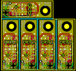
Let’s say you really wanted to make a whole bunch of those Xling open source Tamagotchi-like key fobs we saw a couple of weeks back. Using KiKit you can gang up six of the boards at a time, using “mousebites” to keep them together during production but make it easy to separate them after all the components are soldered:

/usr/local/bin/kikit panelize grid --space 3 --gridsize 2 3 --tabwidth 3 --tabheight 3 --htabs 2 --vtabs 1 --mousebites 0.5 1 0.25 --radius 1 Xling/hardware/xling.kicad_pcb xling_panel.kicad_pcb

You can see that the parameters let you set space between the boards, number of boards in the grid, width of the tabs, tab dimensions, number of tabs between boards, and even the radius of the curve where the tabs meet the board. These settings were pulled from the examples page, which demonstrates outcomes for many different settings options.

If you want to give this a try, we suggest installing directly from the repository, as improvements are ongoing and the pip3 version didn’t have all of the options shown in the examples. For us this was as easy as sudo python3 setup.py install and then calling the script with the full path /usr/local/bin/kikit.

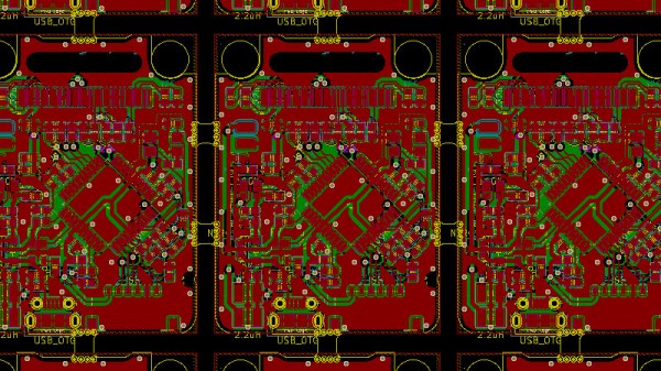
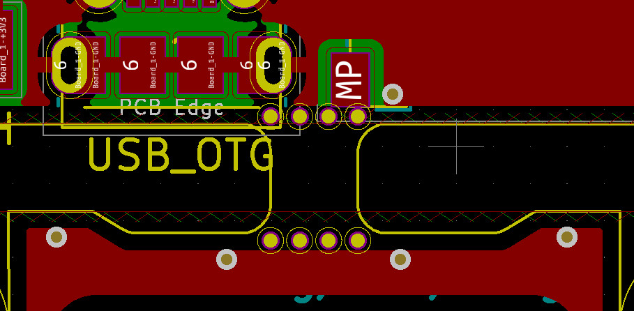
Results from this board are both impressive and cautionary. You can see the top edge of the design is recessed yet the most up-to-date version of KiKit was still able to make the connection. However, how this affects the USB connector on the bottom of the board design may be something to consider before pulling the trigger on your panel order.

Share Your Projects: KiCad Automations And Pretty Renders

I have a pretty large GitHub repository, with all of my boards open-sourced there. Now, I’m finally facing the major problem it has – it can be uncomfortable for others to work with. I don’t store Gerber files in the repository because that will interfere with how Git functions – you’re supposed to only have source files in the repo. Yet, when someone needs Gerbers for my PCB, or a schematic PDF, or just to see how the board looks before they clone the entire repository, I often don’t have a good option for them.

In my experience as a hacker, being able to find others’ PCBs on GitHub is simply wonderful, but a PCB repository without a README feels barren, and a PCB README without pictures makes me sad. On the other hand, not having these files autogenerate is uncomfortable – updating a picture every time is a major drawback in particular.

Let’s take a look at some KiCad Git integrations, and see what they have to offer.

kicad_cli

We’ve mentioned kicad_cli back when KiCad 7 got released, and in the recently released KiCad 8, it’s only become more powerful. Before, it could do gerbers and schematic PDFs, but now, it can even do DRC checks – which is ideal if you want to add a hook for any pull requests you might encounter.

Continue reading “Share Your Projects: KiCad Automations And Pretty Renders”

Let KiCad And Python Make Your Coils

We like to pretend that our circuits are as perfect as our schematics. But in truth, PCB traces have unwanted resistance, capacitance, and inductance. On the other hand, that means you can use those traces to build components. For example, it isn’t uncommon to see a very small value current sense resistor be nothing more than a long PC board trace. Using PC layers for decoupling capacitance and creating precise transmission lines are other examples. [IndoorGeek] takes us through his process of creating coils on the PCB using KiCad. To help, he used a Python script that works out the circles, something KiCAD has trouble with.

The idea is simple. A coil of wire has inductance even if it is a flat copper trace on a PCB. In this case, the coils are more for the electromagnetic properties, but the same idea applies if you wanted to build tuned circuits. The project took inspiration from FlexAR, an open-source flexible PCB magnet.

Continue reading “Let KiCad And Python Make Your Coils”

Panelizing Boards In KiCad

Panelization of printed circuit boards is a very helpful trick for any PCB design tool to have. By panelizing boards, you can get them ready for automated assembly. You can put testing rigs right on the panel. You can combine different boards to reduce your PCB production cost. But Eagle, Fritzing, and KiCad don’t have proper panelization tools, only hacks and third-party tools to get something close to proper panelization. [Flemming] just created a new utility for KiCad that makes multiple copies of a board connected via mouse bites. It’s not complete panelization functionality, but for a lot of us, it’ll be good enough.

The video demo for this utility (try not to click on that because we’re going to blow some bandwidth with this link) starts off by importing a board into Pcbnew, making several copies of the board, arranging these boards to have 3-4mm spacing, and drawing ‘hint lines’ for the script, telling it where the mouse bites should go. The script runs, and boom, mouse bites and a panel.

This is a KiCad specific tool, and we’ve seen other tools for KiCad that make multiple copies of a board. We’ve also seen tools that take raw Gerbers of multiple designs and turn them into a panel. [Flemming]’s efforts are the closest we’ve seen to having all the features you want out of a panelization utility bild exclusively for KiCad.

While this tool will give you a set of Gerbers with multiple copies of a board connected with mouse bites, this is not in any way a complete solution to panelizing PCBs. If you’re panelizing PCBs, you’ll want to add fiducials in the corners of the full panel, which this tool does not allow you to do. You might want to have one complete ‘frame’ as a panel — effectively a rectangular piece of fiberglass that holds all your PCBs — which this tool does not allow you to do. Since you don’t get a frame, it’s impossible to run programming or testing signals to the frame that would be needed for assembly, but not necessary in production. That said, unless you’re going to spend thousand on Altium or use Open tools that have critical flaws such as GerberPanelizer, this is the best option you’ve got.

Automated PCB Panelization

panel

Some PCB production houses – Seeed Studio and itead studio, especially – allow you to upload a gerber file and receive a printed circuit board very inexpensively. The pricing structure for these board houses is based on predesignated board sizes – 5cm square or 5×10 cm – and sometimes a project is just too small to justify buying a full 25 square centimeters of board. This is where panelizing comes in: by putting multiple copies of a circuit board on one of the available sizes you can get more boards for the same amount of money. But how to panelize your boards without the (sometimes) hassle of cutting and pasting?

[Martin] came up with a way of panelizing PCBs with just a Python script. By creating one copy of a circuit board in KiCAD, he can fire up his script and tell the computer exactly how to duplicate his circuit to fit any size board.

By his own admission, [Martin]’s script is still a little clunky, but it does allow him to edit the panelized board in KiCAD and also copies the nets so the ratsnest doesn’t go between boards.

Improved Part Searches For JLCPCB Parts

Finding the JLCPCB component parts library frustrating to navigate, [Jan Mrázek] took matters into his own hands and made an open-source parametric search utility. We’ve all probably wasted time before trying to track down a particular flavor of a part, and this tool promises to make the process easier.  It downloads data from the JLCPCB parts site upon initialization and presents the user with typical selection filters for categories and parameter values. You can install it yourself on GitHub Pages, or [Jan] provides a link to his site.

For the curious, the details of how to pull parts information from the JLBPCB site can be found in the project’s source code.  We like it when a distributor provides this level of access to their part details and parameters, allowing others to sort and filter the parts in ways not originally envisioned by the site design team.  We think this is a win-win situation — distributors can’t sell parts that designers can’t find.

If [Jan]’s name sounds familiar, it should be.  We have written about several of his projects before, two of them are also PCB designer tools ( KiCad Board Renderings and KiCad Panelization ).

Panelize PCBs Graphically With Hm-panelizer

When you’re working with PCBs and making single units to knock out in those Chinese fabs, going from layout to manufacturable Gerber files is just a few button presses, no matter what PCB layout tool you prefer. But, once you get into producing sets of PCBs that form a larger system, or are making multiple copies for efficient manufacturing, then you’re not going to get far without delving into the art of PCB panelization. We’ve seen a few options over the years, and here’s yet another one that’s looking quite promising —  hm-panelizer by [halfmarble] is a cross platform Python GUI application, which leverages Kivy, so it should run on pretty well on most major platforms without too much hassle. The tool is early in development, so is restricted to handling only straight PCB edges, with horizontal mouse-bites for now, but we’re sure it will quickly grow more general purpose capabilities given time and support.

In an ideal world, open source tools like KiCAD would have a built-in panelizer, but for now we can dream and hm-panelizer might just be good enough for some people. For more choices on panelizing, checkout our guide to making it easy, and just to muddy the waters here’s another way to do it.