Before the era of digital electronic computers, mechanical analog computers were found everywhere. From the relative simplicity of bomb sights to the complexity of fire control computers on 1940s battleships, all the way to 1950s fighter planes, these mechanical wonders enabled feats which were considered otherwise impossible at the time.
One such system that [Ken Shirriff] looked at a while ago is the Bendix Central Air Data Computer. As the name suggests, it is a computer system that processes air data. To be precise, it’s the mechanism found in airplanes that uses external sensor inputs to calculate parameters like altitude, vertical speed, Mach number and air speed.
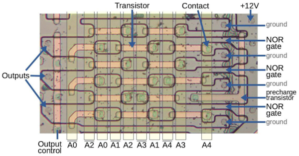
[Ken Shirriff] is looking inside chips again. This time, the subject is the MK4116 — a 16 Kbit DRAM chip. Even without a calculator, you know that’s a whopping 2 Kbytes, and while that doesn’t sound impressive, in the late 1970s, it was a modern miracle.
The chip showed up in computers ranging from the TRS-80 to the Xerox Alto and was even a mainstay of arcade video games. While [Ken] thought it would be a pretty predictable teardown, he found several surprises.
Static RAM chips use flip flops and retain their state as long as power is on. That’s convenient, but each flip flop takes multiple transistors, so there is a limit to how many bits you can put on a particular size chip. Dynamic RAM increases that limit because it is nothing more than a capacitor and a single transistor. This increases memory density, but the problem is that the capacitor doesn’t hold charge indefinitely. The computer or an associated circuit had to refresh the memory periodically to maintain the contents.
One of the key innovations for this chip was the use of multiplexed address lines so it could use a smaller package. Inside, two banks of capacitors store the bits, and, usually, a computer would use eight chips to store a byte. Of course, each memory bit is made to be as compact as possible. This chip is also made to be very low power when idle. The secret is that it doesn’t use load transistors but instead uses an active pull-up tied to the system clock. Another interesting feature is the sense amplifier, which has to measure the tiny noisy voltage from the capacitors.
You’ll see all this and more in [Ken’s] write-up. Chips from that era were relatively easy to take apart compared to today’s devices. Want to know how it’s done? [Ken] can tell you. He is well-known for doing a lot of cool stuff, with ICs and even old mainframe and space hardware.
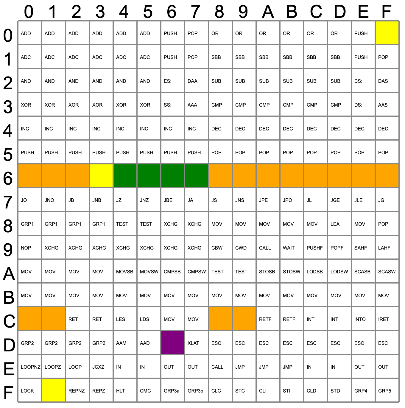
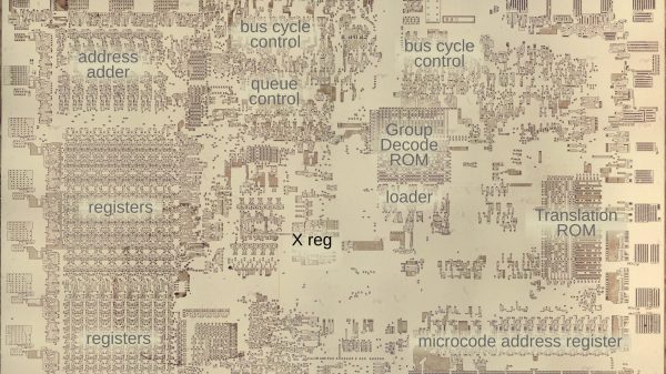
Video gamers know about cheat codes, but assembly language programmers are often in search of undocumented instructions. One way to find them is to map out all of a CPU’s opcodes and where there are holes, try those values, and see what happens. Not good enough for [Ken Shirriff]. He prefers examining the CPU’s microcode and deducing what each part of it does.
Microcode is a feature of many modern CPUs. The CPU runs several “microcode” instructions to process a single opcode. For the Intel 8086, there are 512 micro instructions, each with 21 bits. Each instruction has two parts: a part that moves a source to a destination and another that performs some other operation, such as an ALU operation. [Ken] explains it all in the post, including several hidden registers you can’t see, but the microcode can.
Searching for holes in the opcode table.
Some of the undocumented instructions are probably not useful. They are either impractical or duplicate a function you can already do another way. Not all of the instructions are there for technical reasons. For example, opcode D6, commonly known as SALC for “Set AL to Carry”, seems to exist only as a trap for anyone making a carbon copy of Intel’s microcode. When other companies like NEC made 8086 clones, having an undocumented instruction would strongly suggest they just copied Intel’s intellectual property (in NECs case, they didn’t).
Other cases happen where an instruction just doesn’t make sense. For example, you can pop all segment registers, and though it is not documented, you can deduce that POP CS should be opcode 0F. The problem is there is no sane reason to pop CS off the stack. The instruction works; it just isn’t useful. The opcodes from 60-6F are conditional jumps that are no different from the instructions at 70-7F because of decoding. There is no reason to document both identical instruction ranges.
The plot thickens when you go to two-byte instructions. You’ll find plenty of instructions of dubious value. You don’t hear much about undocumented instructions anymore. Why? Because modern CPUs have enough circuitry to dedicate some to detecting illegal instructions and halting the CPU. But the 8086 was squeezed too tight to allow for such a luxury. Good thing for people like us who enjoy solving puzzles.
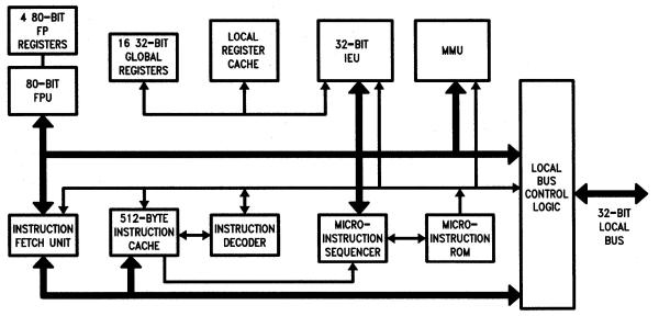
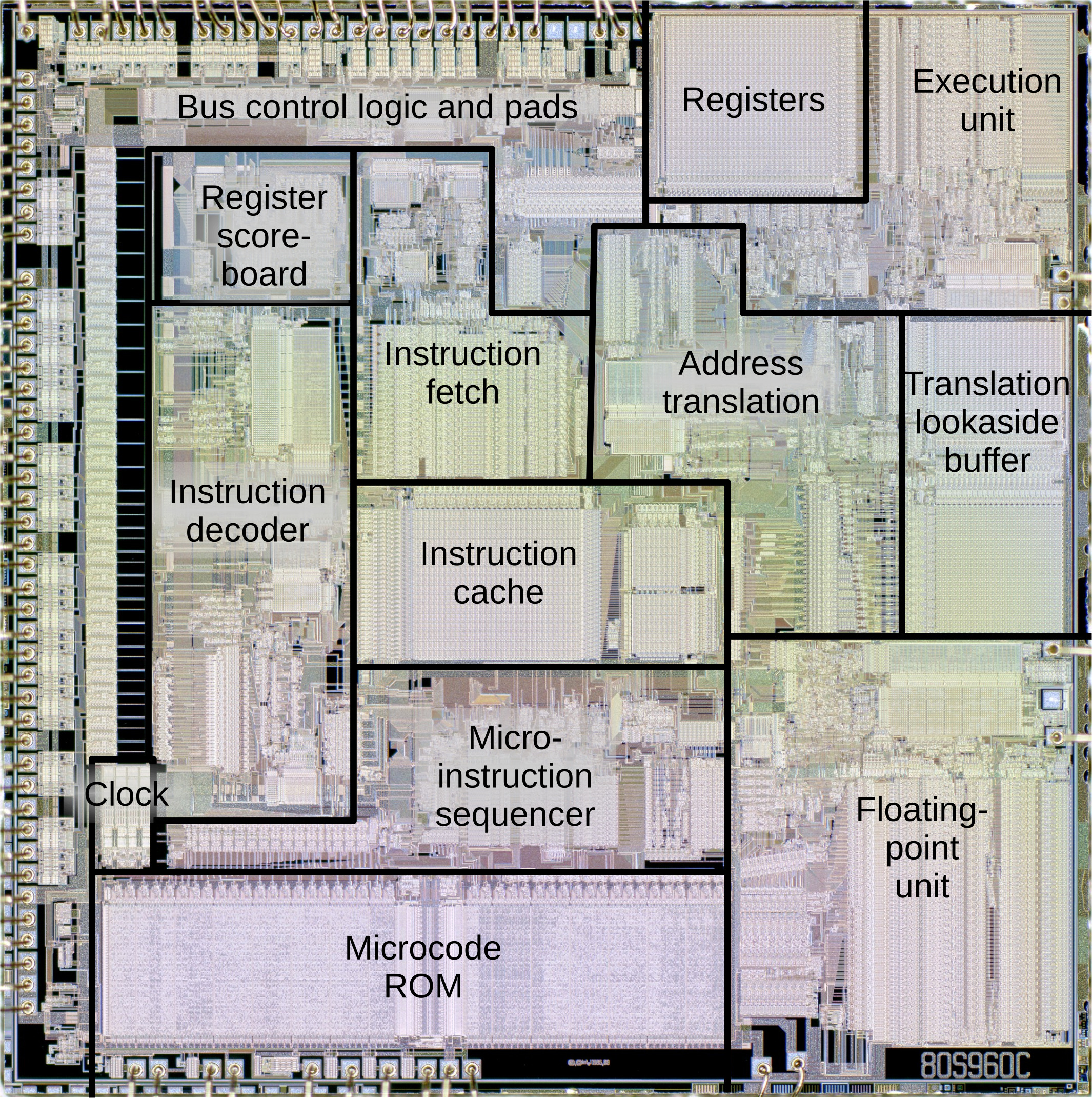
The i960 KA/KB/MC/XA with the main functional blocks labeled. Click this image (or any other) for a larger version. Die image courtesy of Antoine Bercovici. Floorplan from The 80960 microprocessor architecture.
From the consumer space it often would appear as if Intel’s CPU making history is pretty much a straight line from the 4004 to the 8080, 8088 and straight into the era of Pentiums and Cores. Yet this could not be further from the truth, with Intel having churned through many alternate architectures. One of the more successful of these was the Intel i960, which is also the topic of a recent article by [Ken Shirriff].
Remarkably, the i960 as a solid RISC (Reduced Instruction Set Computer) architecture has its roots in Intel’s ill-fated extreme CISC architecture, the iAPX 432. As [Ken] describes in his comparison between the i960 and 432, both architectures are remarkably similar in terms of their instruction set, essentially taking what it could from the 432 project and putting it into a RISC-y shape. This meant that although the i960 could be mistaken as yet another RISC CPU, as was common in the 1980s, but integrated higher-level features as well, such as additional memory protection and inter-process communication. Continue reading “The I960: When Intel Almost Went RISC”→
We thought it was time to give the analog side of Hackaday their chance to shine, and what’s the quintessential analog IC? The op amp! Whether you’re doing tricky signal conditioning, analog computations like it’s 1960, or just making music sound good, op amps are at the heart of many designs. This contest, starting right now, is your chance to show off what you can do with a good op amp, or a few.
And for everyone else, here’s your chance to dip your toes into the warm analog waters. Whether you’ve always wanted to build a Chua’s chaos circuit or just to listen to music, there’s probably an op-amp project that will fit your personal bill. All you have to do to enter is set up a project on Hackaday.io, and use the pull-down menu to enter. We welcome shows of op-amp bravado, naturally, but we’re also stoked to see your simple projects that might help our digital friends leave their world of black and white, and enter into the shades of grey.
Thanks to Digi-Key, our sponsor for the challenge, there are three $150 shopping sprees on the line for the winners. And as always, there are some honorable mention categories to help whet your analog whistle, and to give us an excuse to feature a lot of great projects. You’ve got until June 6, to get your entry in, but these aren’t necessarily simple builds, so get going now.
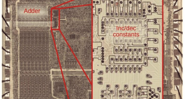
One of the interesting features of the 8086 back in 1978 was the provision for “string” instructions. These took the form of prefixes that would repeat the next instruction a certain number of times. The next instruction was meant to be one of a few string instructions that operated on memory regions and updated pointers to the memory region with each repeated operation. [Ken Shirriff] examines the 8086 die up close and personal to explain how the 8086 microcode pulled this off and it is a great read, as usual.
In general, the string instructions wanted memory pointers in the SI and DI registers and a count in CX. The flags also have a direction bit that determines if the SI and DI registers will increase or decrease on each execution. The repeat prefix could also have conditions on it. In other words, a REP prefix will execute the following string instruction until CX is zero. The REPZ and REPNZ prefixes would do the same but also stop early if the zero flag was set (REPZ) or not set (REPNZ) after each operation. The instructions can work on 8-bit data or 16-bit data and oddly, as [Ken] points out — the microcode is the same either way.
[Ken] does a great job of explaining it all, so we won’t try to repeat it here. But it is more complicated than you’d initially expect. Partially this is because the instruction can be interrupted after any operation. Also, changing the SI and DI registers not only have to account for increment or decrement, but also needs to understand the byte or word size in play. Worse still, an unaligned word had to be broken up into two different accesses. A lot of logic to put in a relatively small amount of silicon.
Even if you never design a microcoded CPU, the discussion is fascinating, and the microphotography is fun to look at, too. We always enjoy [Ken’s] posts on little CPUs and big computers.
The 8086 has been around since 1978, so it’s pretty well understood. As the namesake of the prevalent x86 architecture, it’s often studied by those looking to learn more about microprocessors in general. To this end, [Ken Shirriff] set about reverse engineering the 8086’s multiplication algorithm.
[Ken]’s efforts were achieved by using die photos of the 8086 chip. Taken under a microscope, they can be used to map out the various functional blocks of the microprocessor. The multiplication algorithm can be nutted out by looking at the arithmetic/logic unit, or ALU. However, it’s also important to understand the role that microcode plays, too. Even as far back as 1978, designers were using microcode to simplify the control logic used in microprocessors.
[Ken] breaks down his investigation into manageable chunks, exploring how the chip achieves both 8-bit and 16-bit multiplication in detail. He covers how the numbers make their way through various instructions and registers to come out with the right result in the end.
It’s a fun look at what’s going on at the ground level in a chip that’s been around since before the personal computer revolution. For any budding chip designers, it’s a great academic exercise to follow along at home. If you’ve been doing your own digging deep into CPU architectures, don’t hesitate to drop us a line!