[Ken] Looks At The 386

The 80386 was — arguably — Intel’s first modern CPU. The 8086 was commercially successful, but the paged memory model was stifling. The 80286 also had a protected mode, which differed from the 386’s. [Ken Shirriff] takes the 386 apart for us in a recent blog post.

The 286’s protected mode was less successful than the 386 because of several key limitations as it was a 16-bit processor with a 24-bit address bus. It still required segment changes to access larger amounts of memory, and it had no good way to call back into real mode for compatibility reasons. The 386 fixed all that. You could adopt a segment strategy if you wanted to. But you could also load the segment registers once to point to a 4 GB linear address space and then essentially forget them. You also had a virtual 86 mode that could simulate real mode with some work.

The CPU used a 1-micron process, compared to the 1.5-micron process used earlier. The chip had 285,000 transistors (although the 80386SL had many more). That was ten times the number of devices on the 8086. The cheaper 386SX did use the 1.5 micron process for a while, but with a 16-bit external bus, this was feasible. While 285,000 sounds like a lot, a Core i9 has around 4.2 billion transistors. Times have changed.

A smaller design also allowed chips like the 386SL for laptops. The CPU took up only about a fourth of the die. The rest held bus controllers and cache interfaces to cut costs on laptops. That’s why it had so many more transistors.

[Ken] does his usual in-depth analysis of both the die and the history behind this historic device. We spent a lot of time writing protected mode 386 code, and it was nice to see the details of a very old friend. These days, you can get a pretty capable CPU system on a solderless breadboard, but designing a working 386 system took a few extra parts. The 80286 was a stepping stone between the 8086 and 80386, but even it had some secrets to give up.

This Weekend: Vintage Computer Festival West

Next weekend is the Vintage Computer Festival West, held at the Computer History Museum. Hackaday is once again proud to sponsor this event that brings together the people and hardware that drove the information revolution. [Bil Herd] and [Joshua Vasquez] will be on hand representing the Hackaday Crew.

This year’s talks show an impressive lineup of people. [Bil Herd] will be on stage with a collection of other engineers who secured Commodore’s place in history. The Computer History Museum has a very active restoration program for original computer hardware. Friend of Hackaday, [Ken Shirriff], has been working on a restoration of the Xerox Alto and is on the panel giving a talk about the process. And just to cherry-pick one more highlight, there’s a talk on system debugging before you even turn the thing on — a topic that can save you from having a very bad day with very ancient hardware.

A great part of VCF is that the exhibits are often either hands-on or demonstrations so you can actually play around with hardware which most people have never even seen in person. Add to that the collection at the Computer History Museum plus some extra exhibits they have planned for the event and you’re likely to run out of time before you make your way through everything.

Since we’ve mentioned the Computer History Museum, we also have some upcoming news. A bit later this month, Hackaday Contributor-at-Large [Voja Antonic] has been invited to visit the museum, record his oral history, and deliver to their collection an original Galaksija computer — wildly successful first as a kit and then as a manufactured computer which he built in Yugoslavia 1983. Congratualtions [Voja]!

The Intel 8088 And 8086 Processor’s Instruction Prefetch Circuitry

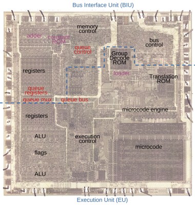
The 8088 die under a microscope, with main functional blocks labeled. This photo shows the chip's single metal layer; the polysilicon and silicon are underneath. (Credit: Ken Shirriff)
The 8088 die under a microscope, with main functional blocks labeled. This photo shows the chip’s single metal layer; the polysilicon and silicon are underneath. (Credit: Ken Shirriff)

Cache prefetching is what allows processors to have data and/or instructions ready for use in a fast local cache rather than having to wait for a fetch request to trickle through to system RAM and back again. The Intel 8088  (and its big brother 8086) processor was among the first microprocessors to implement (instruction) prefetching in hardware, which [Ken Shirriff] has analyzed based on die images of this famous processor. This follows last year’s deep-dive into the 8086’s prefetching hardware, with (unsurprisingly) many similarities between these two microprocessors, as well as a few differences that are mostly due to the 8088’s cut-down 8-bit data bus.

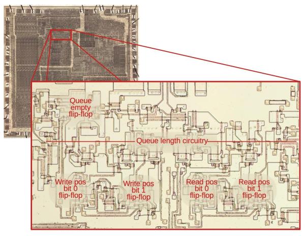
While the 8086 has 3 16-bit slots in the instruction prefetcher the 8088 gets 4 slots, each 8-bit. The prefetching hardware is part of the Bus Interface Unit (BIU), which effectively decouples the actual processor (Execution Unit, or EU) from the system RAM. While previous MPUs would be fully deterministic, with instructions being loaded from RAM and subsequently executed, the 8086 and 8088’s prefetching meant that such assumptions no longer were true. The added features in the BIU also meant that the instruction pointer (IP) and related registers moved to the BIU, while the ringbuffer logic around the queue had to somehow keep the queueing and pointer offsets into RAM working correctly.

Even though these days CPUs have much more complicated, multi-level caches that are measured in kilobytes and megabytes, it’s fascinating to see where it all began, with just a few bytes and relatively straight-forward hardware logic that you easily follow under a microscope.

The 1970s Computer: A Slice Of Computing

What do the HP-1000 and the DEC VAX 11/730 have in common with the video games Tempest and Battlezone? More than you might think. All of those machines, along with many others from that time period, used AM2900-family bit slice CPUs.

The bit slice CPU was a very successful product that could only have existed in the 1970s. Today, if you need a computer system, there are many CPUs and even entire systems on a chip to choose from. You can also get many small board-level systems that would probably do anything you want. In the 1960s, you had no choices at all. You built circuit boards with gates on the using transistors, tubes, relays, or — maybe — small-scale IC gates. Then you wired the boards up.

It didn’t take a genius to realize that it would be great to offer people a CPU chip like you can get today. The problem is the semiconductor technology of the day wouldn’t allow it — at least, not with any significant amount of resources. For example, the Motorola MC14500B from 1977 was a one-bit microprocessor, and while that had its uses, it wasn’t for everyone or everything.

The Answer

The answer was to produce as much of a CPU as possible in a chip and make provisions to use multiple chips together to build the CPU. That’s exactly what AMD did with the AM2900 family. If you think about it, what is a CPU? Sure, there are variations, but at the core, there’s a place to store instructions, a place to store data, some way to pick instructions, and a way to operate on data (like an ALU — arithmetic logic unit). Instructions move data from one place to another and set the state of things like I/O devices, ALU operations, and the like.

Continue reading “The 1970s Computer: A Slice Of Computing”

What’s A Transfluxor?

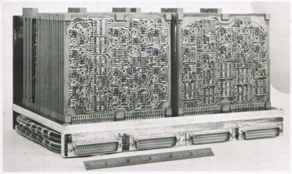
In the 1967 movie The Graduate, a wise older man gives some advice to the title character: plastics. Indeed, plastics would become big business. In 1962, though, a computer-savvy character might have offered a different word: transfluxor. What’s a transfluxor? Well, according to computer history sleuth [Ken Shirriff], it was the heart of a 20-pound transistor computer from Arma. Of course, plastics turned out to be a better bet, but in 1962, the transfluxor seemed to be the wave of the future.

In 1962, most computers were room-sized, but the Arma was “micro” taking up just 0.4 cubic feet — less than an Apple II. It would eventually spawn computers used in ships at sea and airplanes ranging from the Concorde to Air Force One.

Continue reading “What’s A Transfluxor?”

Hackaday Podcast 242: Mechanical Math, KaboomBox, And Racing The Beam

This week, Editor-in-Chief Elliot Williams and Kristina Panos met up from their separate but equally pin drop-quiet offices to discuss the best hacks of the previous week. Well, we liked these one, anyway.

First up in the news, it’s finally time for Supercon! So we’ll see you there? If not, be sure to check out the talks as we live-stream them on our YouTube channel!

Don’t forget — this is your last weekend to enter the 2023 Halloween Hackfest contest, which runs until 9 AM PDT on October 31st. Arduino are joining the fun this year and are offering some spooky treats in addition to the $150 DigiKey gift cards for the top three entrants.

It’s time for a new What’s That Sound, and Kristina was able to stump Elliot with this one. She’ll have to think of some more weirdo sounds, it seems.

Then it’s on to the hacks, beginning with an insanely complex mechanical central air data computer super-teardown from [Ken Shirriff]. We also learned that you can 3D-print springs and things by using a rod as your bed, and we learned whole lot about rolling your own electrolytic capacitors from someone who got to visit a factory.

From there we take a look at a Commodore Datassette drive that sings barbershop, customizing printf, and a really cool dress made of Polymer-dispersed Liquid Crystal (PDLC) panels. Finally we talk about racing the beam when it comes to game graphics, and say goodbye to Kristina’s series on USPS technology.

Check out the links below if you want to follow along, and as always, tell us what you think about this episode in the comments!

Download and savor at your leisure.

Continue reading “Hackaday Podcast 242: Mechanical Math, KaboomBox, And Racing The Beam”

Using Industrial CT To Examine A $129 USB Cable

What in the world could possibly justify charging $129 for a USB cable? And is such a cable any better than a $10 Amazon Basics cable?

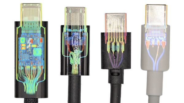
To answer that question, [Jon Bruner] fired up an industrial CT scanner to look inside various cables (Nitter), with interesting results. It perhaps comes as little surprise that the premium cable is an Apple Thunderbolt 4 Pro USB-C cable, which sports 40 Gb/s transfer rates and can deliver 100 Watts of power to a device. And it turns out there’s a lot going on with this cable from an engineering and industrial design perspective. The connector shell has a very compact and extremely complex PCB assembly inside it, with a ton of SMD components and at least one BGA chip. The PCB itself is a marvel, with nine layers, a maze of blind and buried vias, and wiggle traces to balance propagation delays. The cable itself contains 20 wires, ten of which are shielded coax, and everything is firmly anchored to a stainless steel shell inside the plastic connector body.

By way of comparison, [Jon] also looked under the hood at more affordable alternatives. None were close to the same level of engineering as the Apple cable, ranging as they did from a tenth to a mere 1/32nd of the price. While none of the cables contained such a complex PCB, the Amazon Basics cable seemed the best of the bunch, with twelve wires, decent shielding, and a sturdy crimped strain relief. The other cables — well, when you’re buying a $3 cable, you get what you pay for. But does that make the Apple cable worth the expense? That’s for the buyer to decide, but at least now we know there’s something in there aside from Apple’s marketing hype.

We’ve seen these industrial CT scanners used by none other than [Ken Shirriff] and [Curious Marc] to reverse engineer Apollo-era artifacts. If you want a closer look at the instrument itself, check out the video below

Continue reading “Using Industrial CT To Examine A $129 USB Cable”