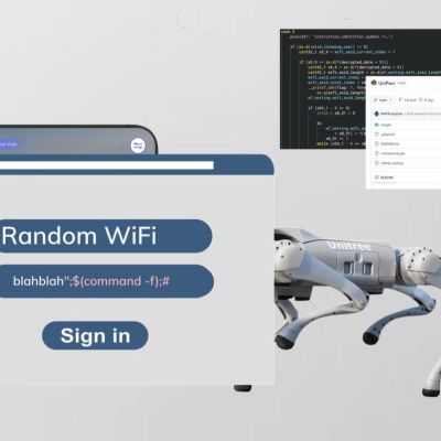
Continuing on his quest to expose the dark underbelly of modern technology, [Benn Jordan] recently did a deep-dive into the rise of so-called robot dogs. Although their most striking resemblance with biological dogs is that they also have four legs and generally follow commands, [Benn] found many issues with them that range from safety issues due to limited sensory capabilities, to basic security vulnerabilities, all the way to suspicious network traffic from Unitree’s robot dog firmware.
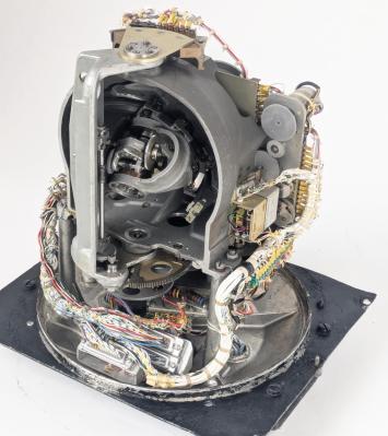
Although not the only seller of this type of quadruped robot, Unitree Robotics has made a name for itself by offering very capable and yet very cheap products. Their basic quadruped robot costs only a few thousand clams and features Lidar and heaps of processing power, all of which should make it a pretty useful device.
Despite this, [Benn] found that the original task that he’d envisioned for the robot, as in protecting his chickens from uninvited visitors, wouldn’t quite work as the robot is rather blind. The reason for this is the placement of the Lidar below the head, which obscures most of what’s behind and around the robot. Rather than risk trampled chickens and chicks, this plan was thus abandoned.
When digging further into the robot, he found an easy to exploit arbitrary command execution flaw via the Wi-Fi password entry field, a year-old CVE-2025-2894 exploit, as well as highly suspicious traffic to Chinese servers whenever the robot’s software figured that it was not being watched. It’s not just their dogs either: UniTree’s humanoid robots are also succeptible.
Although much of this can be circumvented with hacks, issues like the sensory limitations and general distrust of firmware updates makes using these robots a rather daunting and often ill-advised proposition.

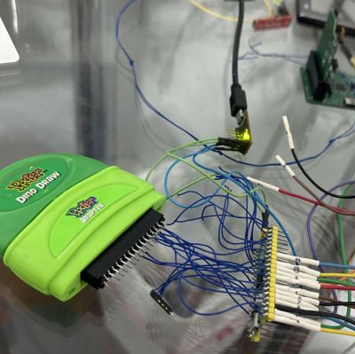 Between 2000 and 2002 the Fisher Price Pixter was sold to children as an educational handheld toy with a touch screen that enabled drawing and listening to music in addition to cartridge-based games and more. It was followed up by multiple new iterations of the system, but as an ecosystem didn’t last beyond 2007. This has left much of the system in obscurity, with people like [Dmitry] doing their best to reverse-engineer, dump and document what they can, such as recently