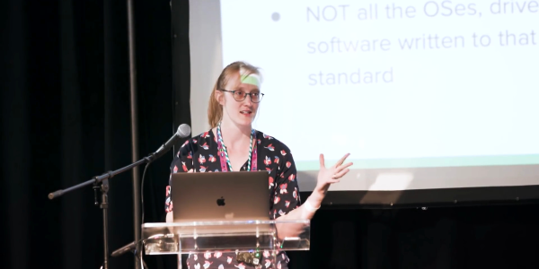
Tim [Mithro] Ansell has a lot to tell you about the current state of open FPGA tooling: 115 slides in 25 minutes if you’re counting. His SymbiFlow project aims to be the GCC of FPGA toolchains: cross-platform, multi-platform, completely free, and all-encompassing. That means that it’s an umbrella framework for all of the work that everyone else is doing, from work on synthesis and verification tools, to placing and routing, to vendor-specific chip libraries. His talk catches you up with the state of the art at the end of 2019, and it’s embedded below. Spoiler alert: SymbiFlow has the big Xilinx 7-series FPGAs in its crosshairs, and is closing in. SymbiFlow is that close to getting a networked Linux system on the FPGA fabric in a Xilinx 7 today, completely independent of any vendor tools.
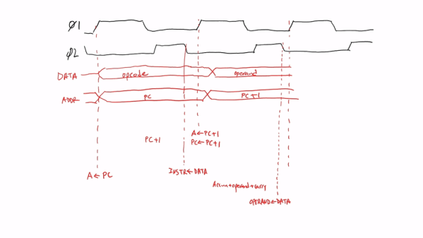
But let’s step back a sec for a little background. When you code for an FPGA, words you type get turned into a bitstream of ones and zeroes that flip perhaps a few million switches inside the chip. Going from a higher-level language to a bitstream is a lot like compiling normal programming languages, except with the twist that the resulting computational logic doesn’t map straight into a machine language, but rather into lower-level physical hardware on the FPGA. So “compilation” for FPGAs involves two steps: synthesis and place-and-routing. Synthesis takes the higher-level language that you write and turns it into a set of networks and timing requirements that represent the same logic, and can work across chip families. Yosys is the open-source synthesis tool of choice here.
Continue reading “Mithro Runs Down Open Source FPGA Toolchains”