Embedding fasteners or other hardware into 3D prints is a useful technique, but it can bring challenges when applied to large or non-flat objects. The solution? Use a gap-cap.
 The gap-cap technique is essentially a 3D printed lid. One pauses a print, inserts hardware, then covers it with a lid before resuming the print. The lid — or gap-cap — does three things. It seals in the part, it fills in empty space left above the component, and it provides a nice flat surface for subsequent layers which makes the whole process much cleaner and more reliable.
This whole technique is a bit reminiscent of the idea of manual supports, except that the inserted piece is intended to be sealed into the print along with the embedded hardware under it.
If you have never inserted anything larger than a nut or small magnet into a 3D print, you may wonder why one needs to bother with a gap-cap at all. The short version is that what works for printing over small bits doesn’t reliably carry over to big, odd-shaped bits.
For one thing, filament generally doesn’t like to stick to embedded hardware. As the size of the inserted object increases, especially if it isn’t flat, it increasingly complicates the printer’s ability to seal it in cleanly. Because most nuts are small, even if the printer gets a little messy it probably doesn’t matter much. But what works for small nuts won’t work for something like an LED strip mounted on its side, as shown here.
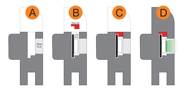
In cases like these a gap-cap is ideal. By pre-printing a form-fitting cap that covers the inserted hardware, one provides a smooth and flat surface that both seals the component in snugly while providing an ideal surface upon which to resume printing.
If needed, a bit of glue can help ensure a gap-cap doesn’t shift and cause trouble when printing resumes, but we can’t help but recall the pause-and-attach technique of embedding printed elements with the help of a LEGO-like connection. Perhaps a gap-cap designed in such a way would avoid needing any kind of adhesive at all.