CPLD Tutorial: Learn Programmable Logic The Easy Way

The guys over at hackshed have been busy. [Carl] is making programmable logic design easy with an 8 part CPLD tutorial. (March 2018: Link dead.  Try the Wayback Machine.) Programmable logic devices are one of the most versatile hardware building blocks available to hackers. They also can have a steep learning curve. Cheap Field Programmable Gate Arrays (FPGA) are plentiful, but can have intricate power requirements. Most modern programmable logic designs are created in a Hardware Description Language (HDL) such as VHDL or Verilog. Now you’ve got a new type of device, a new language, an entirely new programming paradigm, and a complex IDE to learn all at once. It’s no wonder FPGAs have sent more than one beginner running for the hills.

The tutorial cuts the learning curve down in several ways. [Carl] is using Complex Programmable Logic Devices (CPLD). At the 40,000 foot level, CPLDs and FPGAs do the same thing – they act as re-configurable logic. FPGAs generally do not store their configuration – it has to be loaded from an external FLASH, EEPROM, or connected processor. CPLDs do store their configuration, so they’re ready as soon as they power up. As a general rule, FPGAs contain more configurable logic than CPLDs. This allows for larger designs to be instantiated with FPGAs. Don’t knock CPLDs though. CPLDs have plenty of room for big designs, like generating VGA signals.

[Carl] also is designing with schematic capture in his tutorial. With the schematic capture method, digital logic schematics are drawn just as they would be in Eagle or KiCad. This is generally considered an “old school” method of design capture. A few lines of VHDL or Verilog code can replace some rather complex schematics. [Carl’s] simple designs don’t need that sort of power though. Going the schematic capture route eliminates the need to learn VHDL or Verilog.

[Carl’s] tutorial starts with installing Altera’s Quartus II software. He then takes the student through the “hardware hello world” – blinking an LED.  By the time the tutorial is done, the user will learn how to create a 4 bit adder and a 4 bit subtractor. With all that under your belt, you’re ready to jump into big designs – like building a retrocomputer.

[Image via Wikimedia Commons]

Hackaday Links: March 31, 2014

hackaday-links-chain

Wanting to display his Google calendars [Chris Champion] decided to mount an old monitor on the wall. The hack is his installation method which recesses both the bracket and the outlet while still following electrical code (we think).

Since we’re already on the topic. Here’s a hack-tacular project which hangs a laptop LCD as if it were a picture frame. We do really enjoy seeing the wire, which connects to the top corners and hangs from a single hook a few inches above the screen bezel. There’s something very “whatever works” about it that pleases us.

[Jaspreet] build a datalogger in an FPGA. He put together a short video demo of the project but you can find a bit more info from his repo. He’s using a DE0-Nano board which is a relatively low-cost dev board from Terasic.

Want to see what’s under the hood in the processor running a Nintendo 3DS? Who wouldn’t? [Markus] didn’t just post the die images taken through his microscope. He documented the entire disassembly and decapping process. Maybe we should have given this one its own feature?

If you’re streaming on your Ouya you definitely want a clean WiFi signal. [Michael Thompson] managed to improve his reception by adding an external antenna.

We always like to hear about the free exchange of information, especially when it comes to high-quality educational material. [Capt Todd Branchflower] teaches at the United States Air Force Academy. He wrote in to say that his ECE383 Embedded Systems II class is now available online. All the info can also be found at his Github repo.

And finally, do you remember all the noise that was made about 3D printed guns a while back? Well [Mikeasaurus] put together the .iStab. It’s a 3D printed iPhone case with an integrated folding blade…. for personal protection? Who knows. We think it should be a multitasking solution that functions as a fold-down antenna.

A Low Cost Arduino FPGA Shield

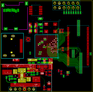
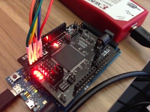
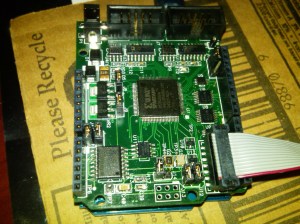
[technolomaniac] is kicking butt over at Hackaday Projects. He’s creating a low cost Arduino based FPGA shield. We’ve seen this pairing before, but never with a bill of materials in the $25 to $30 range. [technolomaniac’s] FPGA of choice is a Xilinx Spartan 6. He’s also including SDRAM, as well as an SPI Flash for configuration. Even though the Spartan 6 LX9 is a relatively small FPGA, it can pack enough punch that the Arduino almost becomes a peripheral. The main interconnect between the two will be the Arduino’s ability to program the Spartan via SPI. Thanks to the shared I/O pins though, the sky is the limit for parallel workflow.

[technolomaniac] spent quite a bit of time on his decoupling schematic. Even on a relatively small FPGA power decoupling is a big issue, especially when high speed signals come into play. Thankfully Xilinx provides guides for this task. We have to mention the two excellent videos [technolomaniac] created to explain his design. Documenting a project doesn’t have to be hours of endless writing. Sometimes it’s just easier to run a screen capture utility and click record. As of this writing, the schematic has just been overhauled, and [technolomaniac] is looking for feedback before he enters the all important layout stage. The design is up on his github repository in Altium format. Due to its high cost, Altium isn’t our first pick for Open Hardware designs. There are free viewers available, but [technolomaniac] makes it simple by putting up his schematic in PDF format (PDF link). Why not head over to projects and help him out?

Continue reading “A Low Cost Arduino FPGA Shield”

Design Your Own Processor With Verilog

Intel-sandy

Designing a computer from scratch is one of the holy grails of hardware design. For programmable logic, designing your own processor is a huge accomplishment. That’s exactly what [zhemao] has done. He created EZ8, an 8 bit processor is written in Verilog. EZ8 has a 3 stage pipeline, which makes design very interesting. Instruction set pipelines have been used in processors for many years. They speed up operation by allowing the processor to execute more than one instruction in parallel. The idea is similar to washing, drying and folding laundry. Most people pipeline their laundry. One load is in the washer, another in the dryer, and a third is being folded. Pipelines aren’t a free lunch though – there are hazards. If one instruction requires the result of an instruction which is still being executed in parallel, there’s a problem. In our laundry analogy this would be like having one sock on the folding table while its mate is still in the dryer. The folding operation must wait for the drying operation to complete before the socks can be paired. This is exactly how assemblers handle the situation – they insert NOPs between known hazard instructions.

[zhemao] didn’t just give us a processor and no support though. He also included an assembler written in OCaml, and an emulator written in C. Several test assembly programs are also up on [zhemao’s] github repo  to verify operation. [zhemao] has tested his processor with Altera Cyclone 5 series FPGAs, but it should be possible to port it to other FPGA manufacturers. If you want more information, [zhemao] also has a discussion going on in the ECE subreddit.

[Thanks for the tip LongHornEngineer!]

[Image courtesy of intel]

A Pick-And-Mix FPGA Retrocomputer

Logo

Cheap FPGA boards are readily available, as are VHDL implementations of classic CPUs like the 6502, 6809, and Z80. Up until now, we haven’t seen anyone take these two parts and combine them into a complete system that turns an FPGA board into a complete 8-bit retrocomputer. Thanks to [Grant]’s work, it’s now possible to do just that (server on fire, here’s a google cache) with a $30 FPGA board and a handful of parts.

In its full configuration, the Multicomp, as [Grant] calls his project, includes either a 6502, 6809, Z80, or (in the future) a 6800 CPU. Video options include either monochrome RCA, RGB VGA, or RGB via SCART. This, along an SD card interface, a PS2 keyboard, and the ability to connect an external 128kB RAM chip (64k available) means it’s a piece of cake to build a proper and complete portable retrocomputer.

What’s extremely interesting about [Grant]’s project is the fact the data and address lines are fully exposed on the FPGA board. This means it’s possible to add whatever circuit you’d like to whatever retrocomputer you can imagine; if you want a few NES gamepads, an IDE interface, or you’d like to design your own primitive video card, it’s just a matter of designing a circuit and writing some assembly.

If you’d like to build your own, search “EP2C5T144C8N” on the usual sites, grab a few resistors and connectors, and take a look at [Grant]’s documentation and upcoming examples.

Via 6502.org forums

Introducing The FleaFPGA Experimenter’s Board

[Valentin] recently tipped us about an FPGA development board he just finished. It is called the FleaFPGA and is aimed to get people interested in the world of Field Programmable Gate Arrays. One of the other reasons that also got [Valentin] to design his own board was that he was frustrated with the existing solutions, them being either too pricey or fairly spare in terms of connectivity.

The main components that you can see in the platform shown above are: a lattice MachX02-7000HE FPGA (6864LUTs), 256Mbits of SDRAM, a USB2.0 host port, a 4096-color VGA connector, a 3.5mm stereo connector, an SD/MMC card slot, a PS/2 keyboard/mouse combo port, a few push buttons and LEDs. An expansion header is also present in order to connect the FleaFPGA to future shields that will be developed. Unfortunately only the board schematics have been released and [Valentin] is currently aiming for a price of $60 per board for <100 quantities. You’ll be able to see a video of the board in action after the break, in which the FPGA has been loaded with a 68000 software core running a variation of the Amiga Juggler Demo.

Continue reading “Introducing The FleaFPGA Experimenter’s Board”

Designing Flip-Flops With Python and Migen

migen

Flip-flops are extremely simple electronic circuits, forming the basis of clock circuits, memory circuits, buffers, and shift registers. Through his dilly-dallying with digital logic, [Jeffrey] decided he would build his own. Not with Verilog or VHDL, though, but Migen: the Python-based way to build digital circuits with software.

Migen is an interesting tool that makes traditional FPGA programming a lot easier; instead of Verilog or VHDL, Migen allows an FPGA to be programmed in Python. Yes, it’s the tool you’ve been waiting for, and the tutorials make it look pretty easy. After installing Migen, [Jeff] wrote a class for a D flip-flop in only three lines of code. That’s three readable lines of code, and he was able to simulate the flip-flop with gtkwave in another two lines. Compared to learning the complexities of VHDL or Verilog, Migen makes digital logic and FPGA programming a breeze.

[Jeff] has a great tutorial for building a D flip-flop with Migen, but we’d love to see some more complex examples of what can be done with this very cool tool. If you’re building (or have built) something with Migen, be sure to send it in and relate your experiences.