A 6502 Overlay Debugger

Retired hardware engineer [Plasmode] recently took on the challenge of building a debugger for the 6502 designed to sit atop the microprocessor while seated in a solder less breadboard. The result is the Diagnostic Overlay for W65C02 Breadboard, consisting of 128 kB SRAM and a 1250-gate CPLD. Except being 0.8 in wide, the overlay debugger is otherwise the same size as the 6502’s 40-pin DIP package, so it doesn’t overhang other portions of your circuit.

Being an initial concept prototype, [Plasmode] mounted the chips dead-bug style on perf board — a process he himself found tiring. If he builds additional debuggers, presumably he will consider making a PCB.

The prototype was constructed using point-to-point soldering with 30-ga wire wrap wire.  It was all done under the inspection microscope.  There are not many connections, but they are rather tedious so I can only do a dozen or so wires per session.  It took me 2 days and several hours total to finish the prototype board.

This design is based on the CRC65 Frugal 6502 Single Board Computer, of course omitting the 6502 itself. Instead of a physical ROM memory chip, he implemented a 64-byte boot loader inside the CPLD and a serial port. This lets him to bootstrap the system over the serial port. He plans on expanding this to include other DIP-packaged retro microprocessors in the future. Check out his Hackaday.io project page ( above ). If you want to dig deeper, he posted the schematics here.

The Orbtrace debugger hardware connected to a development board t hrough a 20-pin ribbon cable. The development board has a green LED shining.

ORBTrace Effort: Open Tool For Professional Debugging

There are some fairly powerful debugging facilities available on today’s microcontrollers — if your code crashes mysteriously, chances are, there’s a debugging interface that could let you track down the exact crash circumstances in no time. Sadly, debugging tools for these powerful interfaces tend to be prohibitively expensive and highly proprietary, thus, not friendly for hobbyists. Now, there’s a community-driven high-capability debugging platform called ORBTrace, brought to us by [mubes] and [zyp].

With parallel trace, you get a constant stream of consciousness, every exact instruction executed by your CPU. [mubes] and [zyp] set out to tap into the power of parallel trace debugging for Cortex-M processors. and the ORBTrace project was born. Relying on the Orbuculum project’s software capabilities, this FPGA-based debugger platform can do parallel trace and the more popular high-speed SWO trace – and way more. ORBTrace has the potential to grow into a powerful debug helper tool, with enough capabilities for anyone to benefit. And of course, it’s fully open-source.

The ORBTrace board, with a FPGA in the center of it, a USB-C connector on the left, and two IDC debug connectors on the right (one ten-pin and one twenty-pin)
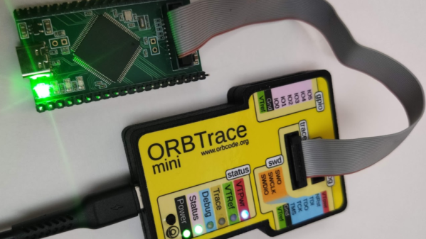
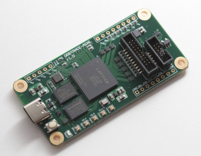
The ORBTrace platform has plenty of untapped potential. There’s the battle-tested JTAG and SWD that you can already use with all the open tools you could expect. However, there’s also plenty of available resources on the FPGA, including even a currently unutilized RISC-V softcore. If you wanted to add support for any other family of devices to this debugger, sky’s the limit! And, of course, there’s cool software to go with it – for example, orbmortem, which keeps a ring buffer of instructions in memory and shows you the last code executed before your CPU stops, or orbstat, a tool for profiling your embedded code.

If you’re looking to purchase effortless feature parity with Segger or Lauterbach devices, the ORBTrace doesn’t promise that. Instead, it’s an open debugging toolkit project, with hardware available for purchase, and software just waiting for you take control of it. This project’s community hangs out in the 1BitSquared discord’s #orbuculum channel, and gateware’s advancing at a rapid pace – welcoming you to join in on the fun.

ORBTrace is a powerful tool for when your goals become large and your problems become complex. And, being a community-driven experimental effort, we’ll undoubtedly see great things come out of it – like the Mooltipass project, originally developed by Hackaday community members, and still going strong.

Unbricking A SEGGER J-Link V9 Debug Probe

Last year [Emil] found themselves in the situation where a SEGGER J-link debug probe suddenly just stopped working. This was awkward not only because in-circuit debuggers are vital pieces of equipment in embedded firmware development, but also because they’re not that cheap. This led [Emil] to take the device apart to figure out what was wrong with it.

After checking voltages on the PCB, nothing obvious seemed wrong. The Tag-Connect style JTAG header on the PCB appeared to be a good second stop, requiring only a bit of work to reverse-engineer the exact pinout and hook up an ST-Link V2 in-circuit debugger to talk with the STM32F205RC MCU on the PCB. This led to the interesting discovery that apparently the MCU’s Flash ROM had seemingly lost the firmware data.

Fortunately [Emil] was able to flash back a version of the firmware which was available on the internet, allowing the J-Link device to work again. This was not the end of the story, however, as after this the SEGGER software was unable to update the firmware on the device, due to a missing bootloader that was not part of the firmware image.

Digging further into this, [Emil] found out a whole host of fascinating details about not only these SEGGER J-Link devices, but also the many clones that are out there, as well as the interesting ways that SEGGER makes people buy new versions of their debug probes.

(Thanks Zelea for the tip)