The Value Of A Worked Example

I was looking over the week’s posts on Hackaday – it’s part of my job after all – and this gem caught my eye: a post about how to make your own RP2040 development board from scratch. And I’ll admit that my first thought was “why would you ever want to do that?” (Not a very Hackaday-appropriate question, honestly.) The end result will certainly cost more than just buying a Pi Pico off the shelf!

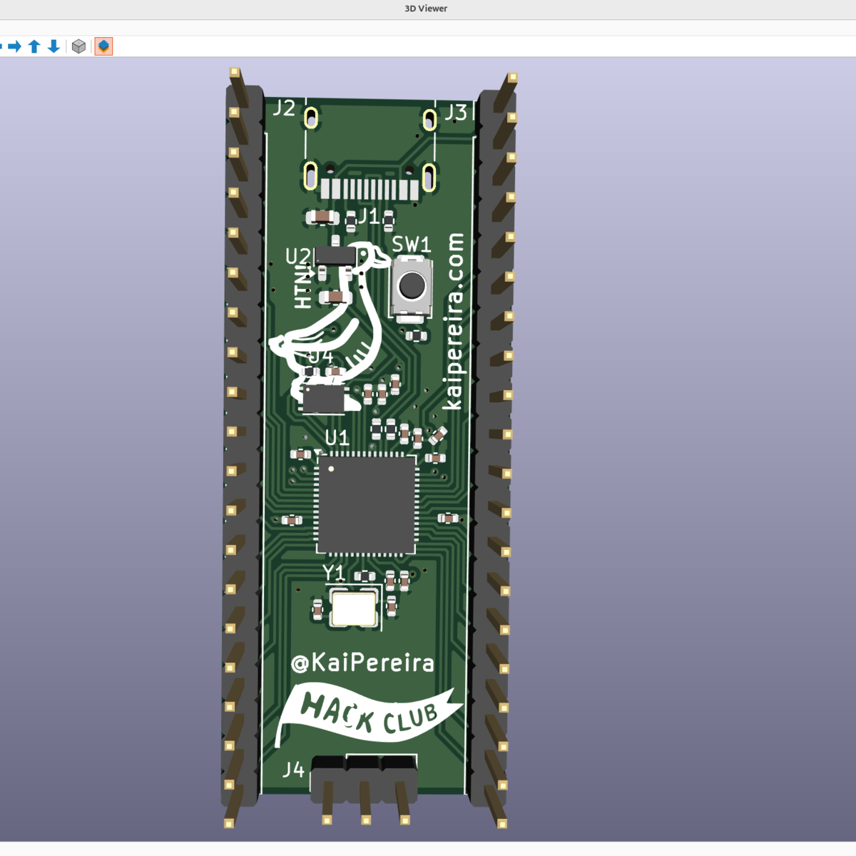
Then it hit me: this isn’t a project per se, but rather [Kai] was using it as an test run to learn the PCB-production toolchain. And for that, replicating a Pico board is perfect, because the schematics are easily available. While I definitely think that a project like this is a bit complicated for a first PCB project – I’d recommend making something fun like an SAO – the advantage of making something slightly more involved is that you run into all of the accompanying problems learning experiences. What a marvelous post-complete-beginner finger exercise!

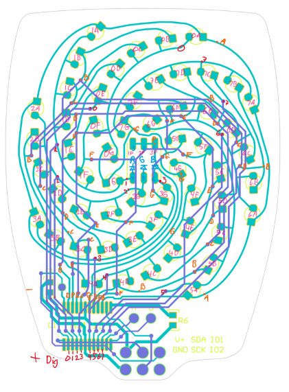
And then it hit me again. [Kai]’s documentation of everything learned during the project was absolutely brilliant. It’s part KiCAD tutorial, part journal about all the hurdles of getting a PCB made, and just chock-full of helpful tips along the way. The quality of the write-up turns it from being just a personal project into something that can help other people who are in exactly the same boat, and I’m guessing that’s a number of you out there.

In the end, this was a perfect Hackaday project. Yes, it was “too simple” for those who have made their 30th PCB design. (Although I’d bet you could still pick up a KiCAD tip or two.) And yes, it doesn’t make economic sense to replicate mass-market devices in one-off. And of course, it doesn’t need that fun art on the board either. But wrap all these up together, and you get a superbly documented guide to a useful project that would walk you through 95% of what you’ll need to make more elaborate projects later on. Superb!

Surely you do “finger exercises” too. Why not write them up, and share the learning? And send them our way – we know just the audience who will want to read it.

DIY RP2040 Dev Board

RP2040 From Scratch: Roll Your Own Dev Board Magic

Have you ever looked at a small development board like an Arduino or an ESP8266 board and thought you’d like one with just a few different features? Well, [Kai] has put out a fantastic guide on how to make an RP2040 dev board that’s all your own.

Development boards are super useful for prototyping a project, and some are quite simple, but there’s often some hidden complexity that needs to be considered before making your own. The RP2040 is a great chip to start your dev-board development journey, thanks to its excellent documentation and affordable components. [Kai] started this project using KiCad, which has all the features needed to go from schematics to final PCB Gerber files. In the write-up, [Kai] goes over how to implement USB-C in your design and how to add flash memory to your board, providing a place for your program to live. Once the crystal oscillator circuit is defined, decoupling capacitors added, and the GPIO pins you want to use are defined, it’s time to move to the PCB layout.

In the PCB design, it starts with an outside-in approach, first defining the board size, then adding the pins that sit along the edges of that board, followed by the USB connector, and then moving on to the internal components. Some components, such as the crystal oscillator, need to be placed near the RP2040 chip, and the same goes for some of the decoupling capacitors. There is a list of good practices around routing traces that [Kai] included for best results, which are useful to keep in mind once you have this many connections in a tight space. Not all traces are the same; for instance, the USB-C signal lines are a differential pair where it’s important that D+ and D- are close to the same length.

Finally, there is a walk-through on the steps needed to have your boards not only made at a board house but also assembled there if you choose to do so. Thanks [Kai] for taking the time to lay out the entire process for others to learn from; we look forward to seeing future dev-board designs. Be sure to check out some of our other awesome RP2040 projects.

Who Is Your Audience?

Here at Hackaday HQ, we all have opinions about the way we like to do things. And no surprise, this extends to the way we like to lay out circuits in schematics. So when we were discussing our own takes on this piece on suggested schematic standards, it was maybe more surprising how much we did agree on than how much we had different preferred styles. But of course, it was the points where we disagreed that provoked the most interesting discussion, and that’s when I had a revelation.

Besides torturing electronics, we all also write for you all, and one thing we always have in mind is who we’re writing for. The Hackaday audience, not to blow you up, is pretty knowledgeable and basically “full-stack” in terms of the hardware/software spectrum. This isn’t to say that everyone is a specialist in everything, though, and we also have certain archetypes in mind: the software type who is just starting out with hardware, the hardware type who isn’t as savvy about software, etc. So, back to schematic layout: Who is your audience? It matters.

For instance, do you organize the pinout for an IC by pin number or by pin function, grouping the power pins and the ADC pins and so on? If your audience is trying to figure out the circuit logic, you should probably go functional. But if you are trying to debug a circuit, you’re often looking at the circuit diagram to figure out what a given pin does, and the pin-number layout is more appropriate.

Do you lay out the logical flow of the circuit in the schematic, or do you try to mimic the PCB layout? Again, it could depend on how your audience will be using it. If they have access to your CAD tool, and can hop back and forth seamlessly from schematic to PCB, the logical flow layout is the win. However, if they are an audience of beginners, or stuck with a PDF of the schematic, or trying to debug a non-working board, perhaps the physical layout is the right approach.

Al Williams, who has experience with projects of a much larger scale than most of us self-taught hackers, doesn’t even think that a schematic makes sense. He thinks that it’s much easier to read and write the design in a hardware description language like VHDL. Of course, that’s certainly true for IC designs, and probably also for boards of a certain complexity. But this is only true when your audience is also familiar with the HDL in question. Otherwise, you’re writing in Finnish for an audience of Spaniards.

Before this conversation, I was thinking of schematic layout as Tom Nardi described it on the podcast – a step along the way to get to the fun parts of PCB layout and then to getting the boards in hand. But at least in our open-source hardware world, it’s also a piece of the documentation, and a document that has an audience of peers who it pays to keep in mind just as much as when I’m sitting down and writing this very newsletter. In some ways, it’s the same thing.

(And yeah, I know the featured image doesn’t exactly fit the topic, but I love it anyway.)

Design Review: LattePanda Mu NAS Carrier

It is a good day for design review! Today’s board is the MuBook, a Lattepanda Mu SoM (System-on-Module) carrier from [LtBrain], optimized for a NAS with 4 SATA and 2 NVMe ports. It is cheap to manufacture and put together, the changes are non-extensive but do make the board easier to assemble, and, it results in a decent footprint x86 NAS board you can even order assembled at somewhere like JLCPCB.

This board is based on the Lite Carrier KiCad project that the LattePanda team open-sourced to promote their Mu boards. I enjoy seeing people start their project from a known-working open-source design – they can save themselves lots of work, avoid reinventing the wheel and whole categories of mistakes, and they can learn a bunch of design techniques/tips through osmosis, too. This is a large part of why I argue everyone should open-source their projects to the highest extent possible, and why I try my best to open-source all the PCBs I design.

Let’s get into it! The board’s on GitHub as linked, already containing the latest changes.

Git’ting Better

I found the very first review item when downloading the repo onto my computer. It took a surprising amount of time, which led me to believe the repo contains a fair bit of binary files – something quite counterproductive to keep in Git. My first guess was that the repo had no .gitignore for KiCad, and indeed – it had the backups/ directory with a heap of hefty .zips, as well as a fair bit of stuff like gerbers and footprint/symbol cache files. I checked in with [LtBrain] that these won’t be an issue to delete, and then added a .gitignore from the Blepis project.

Continue reading “Design Review: LattePanda Mu NAS Carrier”

PCB Design Review: M.2 SSD Splitter

Today’s PCB design review is a board is from [Wificable]. iI’s a novel dual-SSD laptop adapter board! See, CPUs and chipsets often let you split wide PCIe links into multiple smaller width links. This board relies on a specific laptop with a specific CPU series, and a BIOS mod, to put two M.2 NVMe SSDs into a single SSD slot of a specific series’ laptop.

This board has two crucial factors – mechanical compatibility, and electrical function. Looking into mechanics, it’s a 0.8 mm thick PCB that plugs into a M.2 socket, and it has sockets for two SSDs on it – plenty of bending going on. For electronics, it has a PCIe REFCLK clock buffer, that [Wificable] found on Mouser – a must have for PCIe bifurcation, and a must-work for this board’s core! Apart from that, this is a 4-layer board, it basically has to be for diffpairs to work first-try.

Of course, the clock buffer chip is the main active component and the focus of the board, most likely mistakes will happen there – let’s look at the chip first.

Continue reading “PCB Design Review: M.2 SSD Splitter”

Sony Vaio Revived: Power, The Second 80%

A bit ago, I’ve told you about how the Sony Vaio motherboard replacement started, and all the tricks I used to make it succeed on the first try. How do you plan out the board, what are good things to keep in mind while you’re sourcing parts, and how do you ensure you finish the design? This time, I want to tell you my insights about what it takes for your new board revision to stay on your desk until completion, whether it’s helping it not burn up, or making sure the bringup process is doable.

Uninterrupted, Granular Power

Power was generally comfortable to design, but I did have to keep some power budgets in mind. A good exercise for safeguarding your regulators is keeping a .txt file where you log consumers and their expected current consumption on each board power rail, making sure all of your power regulators, connectors, and tracks, can handle quite a bit more than that current. Guideline: increase current by 20%-50% when figuring out the specs for switching regulators and inductors, and, multiply by 10-20% when figuring out conversion losses going between downstream and upstream rails.

I did have a blunder in this department – not accounting for track current early on enough. I laid out the board using 0.5mm wide tracks for power – it looked spacious enough. Then, I put “0.5mm” into a track current calculator and saw a harrowing temperature increase for the currents I was expecting. At that point in routing, it took some time to shift tracks around to accomodate the trace width I actually needed, which is to say, I should’ve calculated it all way way earlier. Thankfully, things went well in the end.

Continue reading “Sony Vaio Revived: Power, The Second 80%”

Supercon 2024 SAO Petal KiCad Redrawing Project

Last week I completed the SAO flower badge redrawing task, making a complete KiCad project. Most of the SAO petals are already released as KiCad projects, except for the Petal Matrix. The design features 56 LEDs arranged in eight spiral arms radiating from the center. What it does not feature are straight lines, right angles, nor parts placed on a regular grid.

Importing into KiCad

Circuit Notes for LEDs, Thanks to [spereinabox]
I followed the same procedures as the main flower badge with no major hiccups. This design didn’t have any released schematics, but backing out the circuits was straightforward. It also helped that user [sphereinabox] over on the Hackaday Discord server had rung out the LED matrix connections and gave me his notes.

Grep Those Positons

I first wanted to only read the data from the LEDs for analysis, and I didn’t need the full Kicad + Python scripting for that. Using grep on the PCB file, you get a text file that can be easily parsed to get the numbers. I confirmed that the LED placements were truly as irregular as they looked.

My biggest worry was how obtain and re-apply the positions and angles of the LEDs, given the irregular layout of the spiral arms. Just like the random angles of six SAO connector on the badge board, [Voja] doesn’t disappoint on this board, either. I fired up Python and used Matplotlib to get a visual perspective of the randomness of the placements, as one does. Due to the overall shape of the arms, there is a general trend to the numbers. But no obvious equation is discernable.

Continue reading “Supercon 2024 SAO Petal KiCad Redrawing Project”