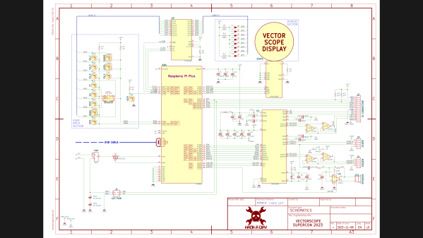
An ATX motherboard sits on a grey surface with the I/O in the foreground. Behind the I/O is a large image of Tux, the Linux penguin, taking up most of the PCB and winding its way around different components on the board. Tux is part of the PCB itself, with his feet, beak, and outline in gold, body in black silkscreen, and belly in green soldermask.

Designing Aesthetically-Pleasing PCBs

We’ve seen our share of custom PCBs here on Hackaday, but they aren’t always pretty. If you want to bring your PCB aesthetics up a notch, [Ian Dunn] has put together a guide for those wanting to get into PCB art.

There are plenty of tutorials about making a functional PCB, but finding information about PCB art can be more difficult. [Ian] walks us through the different materials available from PCB fabs and how the different layer features can affect the final aesthetic of a piece. For instance, while black and white solder mask are opaque, other colors are often translucent and affected by copper under the surface.

PCB design software can throw errors when adding decorative traces or components to a board that aren’t connected to any of the functional circuitry, so [Ian] discusses some of the tricks to avoid tripping up here. For that final artistic flair, component selection can make all the difference. The guide has recommendations on some of the most aesthetically pleasing types of components including how chips made in the USSR apparently have a little bit of extra panache.

If you want to see some more on PCB art, check out this work on full-color PCBs and learn the way of the PCB artist.

The Whole Thing In Python

[hsgw] built a macropad in Python, and that’s not a strange language to choose to program the firmware in these days. But that’s just the tip of the iceberg. The whole process — from schematic capture, through routing and generating the PCB, and even extending to making the case — was done programmatically, in Python.

The macropad itself isn’t too shabby, sporting an OLED and some nice silkscreen graphics, but the whole point here is demonstrating the workflow. And that starts with defining the schematic using skidl, laying out the board with pcbflow, which uses a bunch of KiCAD footprints, and then doing the CAD design for a case in cadquery, which is kind of like OpenSCAD.

The result is that the whole physical project is essentially code-defined from beginning to end.  We’re not sure how well all the different stages of the workflow play together, but we can imagine that this makes versioning a ton easier.  Coding a PCB is probably overkill for something simple like this — you’d be faster to lay it out by hand for sure — but it doesn’t really scale.  There’s definitely some level of complexity where you don’t want to be clicking an pointing, but rather typing. Think of this as the “hello world” to designing in code.

Some of the tools in the workflow were new to us, but if you’d like an in-depth look at cadquery, we’ve got you covered. [Tim Böscke]’s insane CPU made from 555 timers (yes, really) uses pcbflow. And if you’d like to dig back a bit into the origins of Python PCB design, this post introduces CuFlow, on which pcbflow was based.

PCB antenna rendered useless by overly enthusiastic copper fill.

The Many Ways You Can Easily Ruin Your PCB Antenna Design

PCB antenna impaired by copper fill and other attenuation sources.

We have all seen Printed Circuit Board (PCB) antennas: those squiggly bits of traces on PCBs connected often to a Bluetooth, WiFi or other wireless communication chip. On modules like for the ESP8266 and ESP32 platforms the PCB antennas are often integrated onto the module’s PCB, yet even with such a ready-made module it’s possible to completely destroy the effectiveness of this antenna. These and other design issues are discussed in this article by [MisterHW].

It covers a range of examples of poor design, from having ground fill underneath an antenna, to having metal near the antenna, to putting dielectric materials near or on top of the antenna. The effect of all of these issues is generally to attenuate the signal, sometimes to the point where the antenna is essentially useless.

Ultimately, the best PCB antenna design is one where there is no nearby copper fill, and there are no traces running near or on layers below the antenna. After all, any metal trace or component is an antenna, and any dielectric materials will dampen the signal. Fortunately, there is e.g. a free KiCad library with ready-to-use PCB antenna designs to help one get started with a custom design, as well as many other resources, covered in the article.

If you want to get really professional about checking the effectiveness of an antenna design, you’ll want to use a Network Vector Analyzer. These will also help you with tuning the capacitors used with the PCB antenna.

(Featured image: PCB antenna rendered useless by overly enthusiastic copper fill.)

Working With BGAs: Design And Layout

The Ball Grid Array, or BGA package is no longer the exclusive preserve of large, complex chips on computer motherboards: today even simple microcontrollers are available with those little solder balls. Still, many hobbyists prefer to stay with QFP and QFN packages because they’re easier to solder. While that is a fair point, BGA packages can offer significant space savings, and are sometimes the only choice: with the ongoing chip shortage, some other package versions might simply be unavailable. Even soldering doesn’t have to be complicated: if you’re already comfortable with solder paste and reflow profiles, adding a BGA or two into the mix is pretty easy.

In this article we’ll show that working with BGA chips is not as difficult as it may seem. The focus will be on printed circuit board design: how to draw proper footprints, how to route lots of signals and what capabilities your PCB manufacturer should have. We’ll cover soldering and rework techniques in a future article, but first let’s take a look at why BGAs are used at all.

Continue reading “Working With BGAs: Design And Layout”

PCB Thermal Design Hack Gets Hot And Heavy

Thanks to the relatively recent rise of affordable board production services, many of the people reading Hackaday are just now learning the ropes of PCB design. For those still producing the FR4 equivalent of “Hello World”, it’s accomplishment enough that all the traces go where they’re supposed to. But eventually your designs will become more ambitious, and with this added complexity will naturally come new design considerations. For example, how do you keep a PCB from cooking itself in high current applications?

It’s this exact question that Mike Jouppi hoped to help answer when he hosted last week’s Hack Chat. It’s a topic he takes very seriously, enough that he actually started a company called Thermal Management LLC dedicated to helping engineers cope with PCB thermal design issues. He also chaired the development of IPC-2152, a standard for properly sizing board traces based on how much current they’ll need to carry. It isn’t the first standard that’s touched on the issue, but it’s certainly the most modern and comprehensive.

It’s common for many designers, who can be referencing data that in some cases dates back to the 1950s, to simply oversize their traces out of caution. Often this is based on concepts that Mike says his research has found to be inaccurate, such as the assumption that the inner traces of a PCB tend to run hotter than those on the outside. The new standard is designed to help designers avoid these potential pitfalls, though he notes that it’s still an imperfect analog for the real-world; additional data such as mounting configuration needs to be taken into consideration to get a better idea of a board’s thermal properties.

Even with such a complex topic, there’s some tips that are widely applicable enough to keep in mind. Mike says the thermal properties of the substrate are always going to be poor compared to copper, so using internal copper planes can help conduct heat through the board. When dealing with SMD parts that produce a lot of heat, large copper plated vias can be used to create a parallel thermal path.

Towards the end of the Chat, Thomas Shaddack chimes in with an interesting idea: since the resistance of a trace will increase as it gets hotter, could this be used to determine the temperature of internal PCB traces that would otherwise be difficult to measure? Mike says the concept is sound, though if you wanted to get an accurate read, you’d need to know the nominal resistance of the trace to calibrate against. Certainly something to keep in mind for the future, especially if you don’t have a thermal camera that would let you peer into a PCB’s inner layers.

A rig used to test thermal properties of different trace configurations.

While the Hack Chats are often rather informal, we noticed some fairly pointed questions this time around. Clearly there were folks out there with very specific issues that needed some assistance. It can be difficult to address all the nuances of a complex problem in a public chat, so in a few cases we know Mike directly reached out to attendees so he could talk them through the issues one-on-one.

While we can’t always promise you’ll get that kind of personalized service, we think it’s a testament to the unique networking opportunities available to those who take part in the Hack Chat, and thank Mike for going that extra mile to make sure everyone’s questions were answered to the best of his ability.


The Hack Chat is a weekly online chat session hosted by leading experts from all corners of the hardware hacking universe. It’s a great way for hackers connect in a fun and informal way, but if you can’t make it live, these overview posts as well as the transcripts posted to Hackaday.io make sure you don’t miss out.

Remoticon 2021 // Debra Ansell Connects PCB In Ways You Didn’t Expect

“LEDs improve everything.” Words to live by. Most everything that Debra Ansell of [GeekMomProjects] makes is bright, bold, and blinky. But if you’re looking for a simple string of WS2812s, you’re barking up the wrong tree. In the last few years, Debra has been making larger and more complicated assemblies, and that has meant diving into the mechanical design of modular PCBs. In the process Debra has come up with some great techniques that you’ll be able to use in your own builds, which she shared with us in a presentation during the 2021 Hackaday Remoticon.

She starts off with a quick overview of the state of play in PCB art, specifically of the style that she’s into these days: three dimensional constructions where the physical PCB itself is a sculptural element of the project. She’s crossing that with the popular triangle-style wall hanging sculpture, and her own fascination with “inner glow” — side-illuminated acrylic diffusers. Then she starts taking us down the path of creating her own wall art in detail, and this is where you need to listen up. Continue reading “Remoticon 2021 // Debra Ansell Connects PCB In Ways You Didn’t Expect”

The Benefits Of Critiquing Your Own PCB Designs

In a recent retrospective video, [Phil] from Phil’s Lab goes through a number of his early PCB designs, to critique and comment on what he likes and doesn’t like in these designs. Even though it’s only been a few a few years, he founds plenty that’s wrong. From poor and inconsistent formatting in the schematic, to sloppy and outright broken PCB layouts. It’s a fascinating look at years of lessons learned.

[Phil] comments on the importance of clear labeling and organization of sections and pages in the schematic to make it obvious what the function of a block is. Other lessons include the labeling of nets to make PCB routing a lot easier, making good use of PCB planes, getting all relevant information on components and layout in the schematic as a comment, and connecting decoupling capacitors to their relevant pins.

Although we tend to forget about older projects, it can be very interesting to take a look at them now and then, to see (hopefully) our progress over the years. In the case of [Phil] it’s fascinating to see the transition from a basic two-sided board with THT components to multi-layer boards with STM32 MCUs.

Continue reading “The Benefits Of Critiquing Your Own PCB Designs”