PCB Thermal Design Hack Gets Hot And Heavy

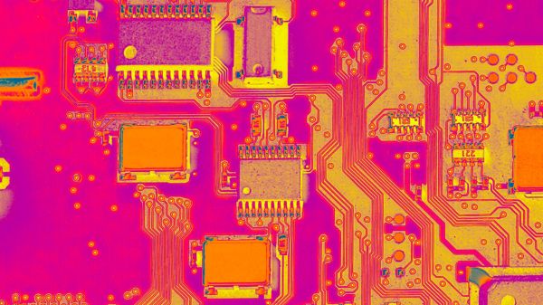
Thanks to the relatively recent rise of affordable board production services, many of the people reading Hackaday are just now learning the ropes of PCB design. For those still producing the FR4 equivalent of “Hello World”, it’s accomplishment enough that all the traces go where they’re supposed to. But eventually your designs will become more ambitious, and with this added complexity will naturally come new design considerations. For example, how do you keep a PCB from cooking itself in high current applications?

It’s this exact question that Mike Jouppi hoped to help answer when he hosted last week’s Hack Chat. It’s a topic he takes very seriously, enough that he actually started a company called Thermal Management LLC dedicated to helping engineers cope with PCB thermal design issues. He also chaired the development of IPC-2152, a standard for properly sizing board traces based on how much current they’ll need to carry. It isn’t the first standard that’s touched on the issue, but it’s certainly the most modern and comprehensive.

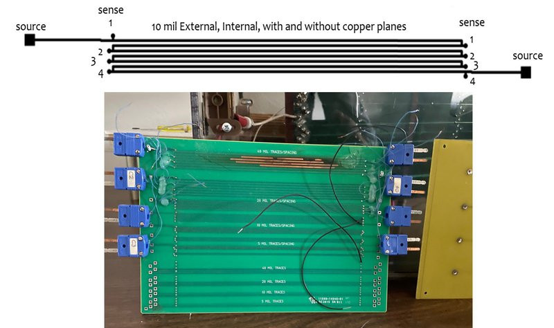
It’s common for many designers, who can be referencing data that in some cases dates back to the 1950s, to simply oversize their traces out of caution. Often this is based on concepts that Mike says his research has found to be inaccurate, such as the assumption that the inner traces of a PCB tend to run hotter than those on the outside. The new standard is designed to help designers avoid these potential pitfalls, though he notes that it’s still an imperfect analog for the real-world; additional data such as mounting configuration needs to be taken into consideration to get a better idea of a board’s thermal properties.

Even with such a complex topic, there’s some tips that are widely applicable enough to keep in mind. Mike says the thermal properties of the substrate are always going to be poor compared to copper, so using internal copper planes can help conduct heat through the board. When dealing with SMD parts that produce a lot of heat, large copper plated vias can be used to create a parallel thermal path.

Towards the end of the Chat, Thomas Shaddack chimes in with an interesting idea: since the resistance of a trace will increase as it gets hotter, could this be used to determine the temperature of internal PCB traces that would otherwise be difficult to measure? Mike says the concept is sound, though if you wanted to get an accurate read, you’d need to know the nominal resistance of the trace to calibrate against. Certainly something to keep in mind for the future, especially if you don’t have a thermal camera that would let you peer into a PCB’s inner layers.

A rig used to test thermal properties of different trace configurations.

While the Hack Chats are often rather informal, we noticed some fairly pointed questions this time around. Clearly there were folks out there with very specific issues that needed some assistance. It can be difficult to address all the nuances of a complex problem in a public chat, so in a few cases we know Mike directly reached out to attendees so he could talk them through the issues one-on-one.

While we can’t always promise you’ll get that kind of personalized service, we think it’s a testament to the unique networking opportunities available to those who take part in the Hack Chat, and thank Mike for going that extra mile to make sure everyone’s questions were answered to the best of his ability.


The Hack Chat is a weekly online chat session hosted by leading experts from all corners of the hardware hacking universe. It’s a great way for hackers connect in a fun and informal way, but if you can’t make it live, these overview posts as well as the transcripts posted to Hackaday.io make sure you don’t miss out.

High-Speed PCB Design Hack Chat With Bil Herd

Join us on Wednesday, September 25 at noon Pacific for the High-Speed PCB Design Hack Chat with Bil Herd!

Printed circuits have become so commoditized that we seldom think much about design details. EDA software makes it easy to forget about the subtleties and nuances that make themselves painfully obvious once your design comes back from the fab and doesn’t work quite the way you thought it would.

PCB design only gets more difficult the faster your circuit needs to go, and that’s where a depth of practical design experience can come in handy. Bil Herd, the legendary design engineer who worked on the Commodore C128 and Plus4/264 computers and many designs since then, knows a thing or two in this space, and he’s going to stop by the Hack Chat to talk about it. This is your chance to pick the brain of someone with a wealth of real-world experience in high-speed PCB design. Come along to find out what kind of design mistakes are waiting to make your day miserable, and which ones can be safely ignored. Spoiler alert: square corners probably don’t matter.

join-hack-chatOur Hack Chats are live community events in the Hackaday.io Hack Chat group messaging. This week we’ll be sitting down on Wednesday, September 25 at 12:00 PM Pacific time. If time zones have got you down, we have a handy time zone converter.

Click that speech bubble to the right, and you’ll be taken directly to the Hack Chat group on Hackaday.io. You don’t have to wait until Wednesday; join whenever you want and you can see what the community is talking about. Continue reading “High-Speed PCB Design Hack Chat With Bil Herd”

Fail Of The Week: When The Epoxy-Coated Chip Is Conductive

Every once in a while, you’ll find some weirdness that will send your head spinning. Most of the time you’ll chalk it up to a bad solder joint, some bad code, or just your own failings. This time it’s different. This is a story of weirdness that’s due entirely to a pin that shouldn’t be there. This is a package for an integrated circuit that has a pin zero.

The story begins with [Erich] building a few development boards for the Freescale Kinetis K20 FPGA. This is a USB-enabled microcontroller, and by all accounts, a worthwhile effort. So far, so good. The problem with the prototype boards was soon apparent. On some of the boards, the external 32 kHz oscillator was not starting. Resoldering the oscillator or microcontroller sometimes solved the problem, but not always. This is troubling, because that means the issue isn’t code, and it’s not the PCB. This is going to take a deep dive and a good inspection microscope.

One of [Erich]’s friends, [Christian B] somehow found the problem. When the Freescale K40 is manufactured, the die is carefully laid in a chip carrier and coated with epoxy, putting it in a small QFN package. The problem is, there’s an extra connection sticking out of one corner of this chip. This is just an artifact of the chip carrier, but if you leave exposed metal connected to ground, something is eventually going to go wrong.

The best guess [Erich] has is that this additional connection is from the manufacturing and packaging process, with the exposed metal pad in this application being bridged to an adjacent pad. Now, if there’s one failure to [Erich]’s design, it’s that the trace comes out of the pin on the adjacent pad at 90 degrees; this isn’t a best practice, but most of the time you can get away with it. This time, though, somebody got burned.

We don’t know how [Christian] ever found this issue. When you look at a tiny QFN package, you don’t expect there to be an extra pin attached to ground that can be easily bridged with a bit of solder paste. It’s either a lot of luck or skill to find this problem, but it’s a great example of the weird things you have to look out for.

Chemistry And Lasers Turn Any Plastic Surface Into A PCB

On the face of it, PCB production seems to pretty much have been reduced to practice. Hobbyists have been etching their own boards forever, and the custom PCB fabrication market is rich with vendors whose capabilities span the gamut from dead simple one-side through-hole boards to the finest pitch multilayer SMD boards imaginable.

So why on Earth would we need yet another way to make PCBs? Because as [Ben Krasnow] points out, the ability to turn almost any plastic surface into a PCB can be really handy, and is not necessarily something the fab houses handle right now. The video below shows how [Ben] came up with his method, which went down a non-obvious path that was part chemistry experiment, part materials science. The basic idea is to use electroless copper plating, a method of depositing copper onto a substrate without using electrolysis.

This allows non-conductive substrates — [Ben] used small parts printed with a Formlabs SLA printer — to be plated with enough copper to form solderable traces. The chemistry involved in this is not trivial; there are catalysts and surfactants and saturated solutions of copper sulfate to manage. And even once he dialed that in, he had to figure out how to make traces and vias with a laser cutter. It was eventually successful, but it took a lot of work. Check out the video below to see how he got there, and where he plans to go next.

You’ve got to hand it to [Ben]; when he decides to explore something, he goes all in. We appreciate his dedication, whether he’s using candles to explore magnetohydrodynamics or making plasma with a high-speed jet of water.

Continue reading “Chemistry And Lasers Turn Any Plastic Surface Into A PCB”

A Touch Scroll Wheel Via OpenSCAD

touch

Recent experiments with the Arduino CapSense library led [Bryan] around the Internet looking for interesting applications. He hit upon a very cool touch scroll wheel made entirely with PCB traces, but the geometry – three interleaved zig zags is impossible to build in the decidedly ungeometric Eagle PCB package. One thing leads to another and now [Bryan] has a cap touch wheel Eagle part designed entirely in OpenSCAD.

The touch scroll wheel implementation [Bryan] found came from an ST touch controller datasheet and used oddly-shaped patterns to create a capacities sensor. Eagle is terrible for designing anything that isn’t laid out at a 45 degree angle, so he fired up OpenSCAD to draw these triangles. Importing into Eagle was another challenge, but a quick Ruby script to convert a DXF file into a set of coordinates for Eagle’s POLYGON command made everything very easy.

If OpenSCADing touch sensors isn’t your thing, there’s also an Eagle library full of them – something we found last week.