Cheap, high-quality PCBs are truly a wonder of our age. That a professionally fabricated board with silkscreen and solder mask can be ordered online and delivered to your door has lowered the bar between a hobbyist project and a polished product. But the wait can be agonizing, and it can throw a wrench into the iterative design process. What to do?
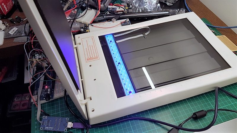
[Andras Kabai] knows the answer to that, and this former flatbed scanner turned into a UV exposer is the centerpiece of his DIY board fab. The old Mustek scanner was a couple of bucks secondhand, and provided not only the perfect form-factor for a board scanner but a trove of valuable parts to reuse. [Andras] replaced the original fluorescent light bar with a long, narrow PCB stuffed with UV LEDs, and added an Arduino Mega to control the original stepper drive. The project looks like it went through a little feature creep, with an elaborate menu system and profiles that include controls for exposure time, the brightness of the LED array via PWM, and the length of board that gets exposed. It’s clearly a work in progress, but early results are encouraging and we’ll be watching to see how [Andras]’ in-house fab shapes up.
This approach to PCB fab is only one of many, of course. You can turn a budget 3D-printer into a PCB machine, or even use an LCD to mask the boards during exposure. The latter intrigues us — an LCD mask and a scanning UV light source could make for a powerful PCB creation tool.


Still waiting for someone to solve the plates through hole problem. Sure there are various drill holes, fill with {graphine, graphite,etc}, electroplate, then etch, or fill with wire and solder, but that’s more aggravating than the wait for boards from Asia and a pain at RF frequencies.
I wouldn’t call it “solved”, but the copper ferrule things are pretty much the best method that I’ve found. Beats waiting, anyway.
No comment on RF performance.
You don’t.. learn how to make copper rivets from wire.
I did it once. And it was impossible to insert the component pins into this holes afterwards :-)
No, this is no adequate substitute for plated through holes.
if the holes you want to use for connecting the two sides are used to put component pins in there anyways (as opposed to just a via), then one often practical solution is to use the component pins AS the through-hole connection by soldering them from both sides. Of course that only makes sense if the following conditions are met:
* you are soldering the components by hand (as opposed to e.g. wave soldering)
* you can actually access the pin with a soldering tip from the component side (i.e. works fine for most stuff but not for stuff where the pin is completely hidden beneath the package such as relays, transformers, big capacitors etc.)
* you don’t need too many of those holes to be used as such a through-hole connection WITH a component pin, because if you have to hand-solder 100 pins from both sides instead of just one, it would be annoying
Solder mask with solder paste.
That’s the reason I have not used my PCB exposure lamp for many years. I converted an old high pressure mercury sunlamp with fluorescent ballasts for this purpose. Originally it used the IR radiators as resistive ballast.
The Quartz lamp produced so much ozone (and probably oxides of nitrogen) during operation that I preferred to leave the room instead of exposing myself to the radiation. But it was good for erasing EPROMs.
Me too… took a scanner body, added some adhesive privacy foil on the inside to refract the light and fitted 3 philips sun tan lamps inside. Did the job perfectly so far. The problem remains etching, I tend to get underetching with the smallest traces.
Most scanners use a glass bed? If so, wouldn’t it block most of the UV spectrum?
No – it’s long-wave UV, not affected much by glass
I’ve never understood why people spend time doing complicated stuff like this when a couple of insect-killer fluorescent tubes will do the job just fine.
So will sunlight…
But I have a gutted scanners, a handful of UV LEDs and the drive to overengineer a solution and I don’t understand why, but I’ll do it anyway
Sunlight is not available anytime But otherwise I would make a non moving LED array for exposure.
What I would like to build (if I had more time and a useful method for plated through holes) would be a laser exposer. Convert the laser unit of an old laser printer with the 400nm diode of a BluRay burner and mount that on the sled of a scanner. Then you could do direct exposure without a transparency.
If i remember correctly an similar Project exists where someone mounted a scanning laser to a moving gantry. Fitting the mechanism from a Laser printer inside a scanner sled should be a very tight fit at best. Also in case of a mask-less procedure the glass plate becomes superfluous, I suspect a design without it would be superior.
A $10 eBay “Nail UV lamp” works fine for me. Only downside is that eBay will recommend you all kinds of manicure products for a few months after the purchase.
I’m glad I got mine at Goodwill then.
Why would you want to PWM it?
PWM should be used to fine tune the UV light “strength” for the given job. e.g. too powerful light could mess up the result if you printed mask is not totally black or could not fully isolate the light.
on the other hand solder mask might need more light, so using PWM you have a chance to adjust it to the given job.
To change the UV Intensity. Exposure is classically measured as exposure time at constant intensity; wich is just a way of setting the amount of energy used to develop the resist, for the sake of repeatable results. Just that in case of Flourescent light, intensity changes with age and temperature (read sequential runs). LEDs dont have that problem, as good ones age so slow that a home gamer should never run into that problem. A constant current source takes care of Temp dependace. This overengineered solution here now can influence exposure energy with variable stepper speed (exposure time really) and also variable UV intensity. A less overengineered solution could do with one of the two. Speaking from experience (i use a non-dimmable UV LED source in a very similar setup) i can tell you that variable exposure time works good. Afterthought: would lower UV intensity not equate an overall slower process?
Of course it would (only) equate an overall slower process. Maximum power for the necessary time and nothing else.
Do you also “scan” or do you use a stionary light source. After all scanning in this case is only a mechanical distribution of the light energy. If I distribute the LEDs over the whole exposure area I don’t need a drive.
The only advantage of the scanning is that you could save some seconds when you expose small PCBs. But that doesn’t seem worth the hassle.
Also scanning. A lot of LED’s equates high cost; an old Scanner of is cheaper than another row of LED’s.
taking that idea one step further would be to scan a single diode in both directions (XY) instead of scanning a line in one direction. that would also have the advantage of allowing to use a diode with a much smaller beam angle (ideally a UV laser diode + collimator lens for a quasi-parallel output) and thus have much better accuracy for small lines and much less “undercutting”. Should be easy to just mount a cheap UV laser diode with a laser pointer collimator lens onto any 3d printer to do the 2d scanning.
Of course, the even cooler way would be to skip the transparency film altogether and use a focused UV beam instead to directly selectively expose the gerber image onto the pcb. but that would require way more work than just dumb 2d 2D-scanning a cheap parallel UV light source over the pcb surface.
You use a PWM to drive LED’s for an average current setup. Average current is basically constant brightness, and it’s easier and more efficient than a constant current setup.
This is a common misconception. LEDs are more efficient at lower current because they run cooler. Part of the losses is resistive, the diode voltages increases with current, the light output is under proportional to the current. So a higher peak current increases your I²R losses. The additional heat decreases the efficiency again.
The only reason for PWM is a very linear brightness modulation, you have to AVOID the higher efficiency of lower currents. You also can avoid the increasing non-uniformity between single LEDs of an array at very low currents.
In this application I would distribute the LEDs over the area with sufficient distance to achieve an even illumination and drive them with one single pulse of a sufficient number of seconds for complete exposure.
Missed it entirely; I was speaking of the conversion circuit itself – PWM is far easier to implement than CC, and is more efficient since you’re not worried about voltage conversions. The LED efficiency is not horribly different in either scenario, provided it’s bypassed with a big enough cap.
I don’t understand it.
You want an exposure energy (power * time). There is no heat issue with LEDs so why in “god’s” sake would you want to stretch the exposure. Maximum power over the necessary time.
Also I don’t see a benefit of the motion, just because you can. Disperse the LED’s over the necessary area and expose.
But that is exactly (half) the Problem. Dispersing the LED’s over the necessary area to get even energy distribution. One tends to end up with a lot of LED’s, for a lot of (often afterwards seldom used) area. If you check Projects which do it like that, design revisions tend to end up with more and more LED’s to get it more even. The other half is good (read powerfull) UV-LED’s are not exactly cheap. Using just 1 or 2 rows of them in an old Scanner is actually an efficient and elegant solution. Exposure time (in my case) for the size of an euro card is well under one minute. A big area of crappy UV-LED’s takes longer while beeing more expensive.
Heat is an issue with LEDs – most of them are only 50%-80% efficient. It’s not a big deal with the 20ma discrete ones, but anything more than 10W needs big passive cooling, and 100W almost needs liquid cooling.
Taking pictures of boards better than most cameras. Heck, there’s even a type of art that uses them.
Nice. I am all on board for reusing and repurposing things.
Do you have a correct link for turning a budget 3d printer into a pcb machine? Sounds interesting. Thanks for the write-up.
Here’s one link: https://hackaday.com/2017/11/27/entry-level-3d-printer-becomes-budget-pcb-machine/
is there a scanner that convert the paper circuits in gerber file?