Earlier this year [Skyhawkson] got ahold of an Apollo-era printed circuit board which he believes was used in a NASA test stand. He took high quality photos of both sides of the board and superimposed them atop each other. After digging into a few obsolete parts from the 1960s, he was able to trace out the connections. I ran across the project just after making schematics for the Supercon badge and petal matrix. Being on a roll, I decided to take [Skyhawkson]’s work as a starting point and create KiCad schematics. Hopefully we can figure out what this circuit board does along the way.
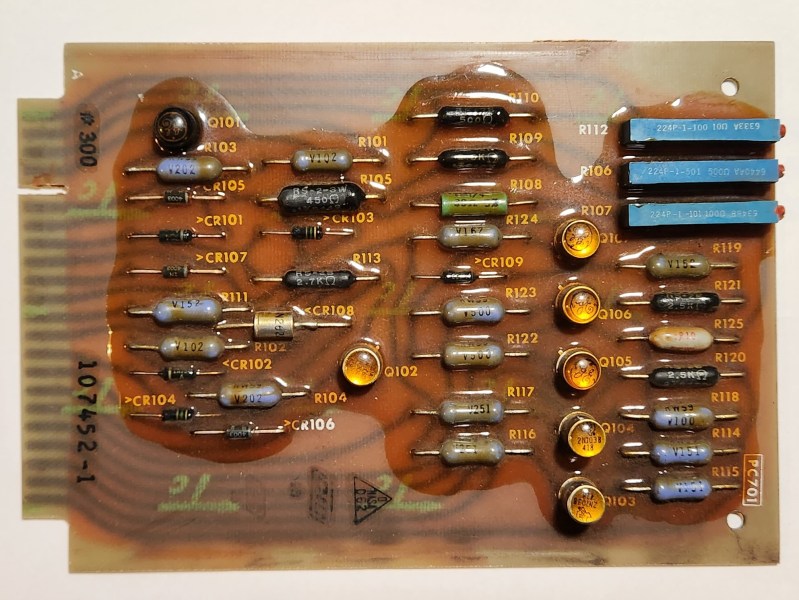
The board is pretty simple:
- approximately 6.5 x 4.5 inches
- 22 circuit edge connector 0.156 in pitch
- 31 ea two-terminal parts ( resistors, diodes )
- 3 ea trimmer potentiometers
- 7 ea transistors
- parts arranged in 4 columns
The first thing I did was to create a “dumb” schematic, with no logical significance other than it matched the geometry of the board. The result should match [Skyhawkson]’s diagrams ( it did ).
The next step was to unwrap the parts and connections, with the goal of making recognizable circuits. It was easy to get circuits crossed up and lose track of the original connections. When making a PCB from schematics, if you delete connections and move parts around, you have the rats nest to guide you. But when going the other way, you’re on your own.
To mitigate this, I made a placeholder PCB whose only purpose is to hold the true netlist. Having a correct PCB design provides a way to check the schematic. Go to the PCB editor, update the PCB from schematics, and run a DRC. I little cumbersome, but better than nothing.
As I first studied the diagram, I realized there are really two independent circuits on the PCB, connected by only one signal. This made unfolding and rearranging the parts easier. Not having any clue what this board did, I just untangled each transistor circuit one by one. Knowing the basic function of a transistor, there are only so many ways to orient each one that makes any sense. Soon, familiar circuits began to appear from the jumble of parts.
Obviously this card belonged in a rack system with an interconnecting back plane. We have no idea what these signals do, and that made it more challenging. In addition, there are some signals that seem unnecessary. My speculation is that these are used in PCB testing, test equipment checkout, or perhaps to operate the board in different modes.
Parts
When researching the parts on the board, [Skyhawkson] found a few that were difficult to pin down. By coincidence, even the sketchy details of two such parts gives us clues to the board’s purpose.
Current Sense Resistor
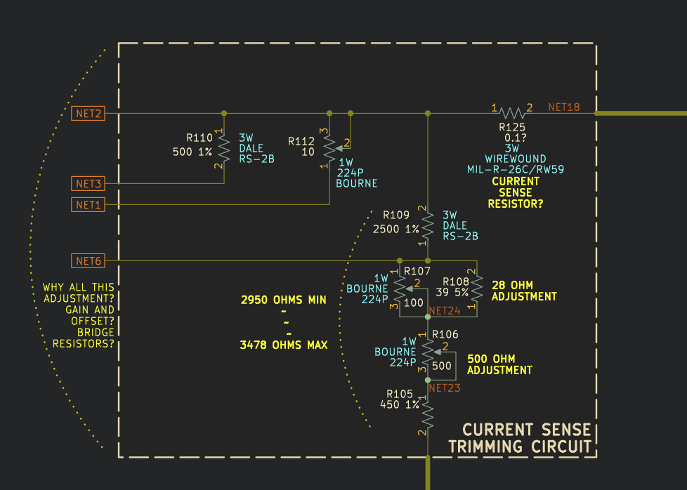
R125 is an X.1 ohm, 3 W wirewound resistor. [Skyhawkson] had to peel back conformal coating to find even a partial part number. This resistor conforms to the MIL-R-26/C, RW59 specification. Many other RWxx resistors from this family are still used today, but RW59 seems to have been dropped a long time ago. It might have already been on the way out back in 1962.
Having such low resistance, perhaps 0.1 ohms, it seems likely to be a current sensing resistor. The high wattage reinforces that idea. But I later realized that almost all of the resistors on the board are 3 W, which I guess was the norm back then. This makes the 3 W power rating of R125 less special. Adding to the mystery, one leg of R125 leaves the board. But lacking a better explanation, I will stick to my initial guess that this is a current sense circuit.
Temperature Compensated Zener
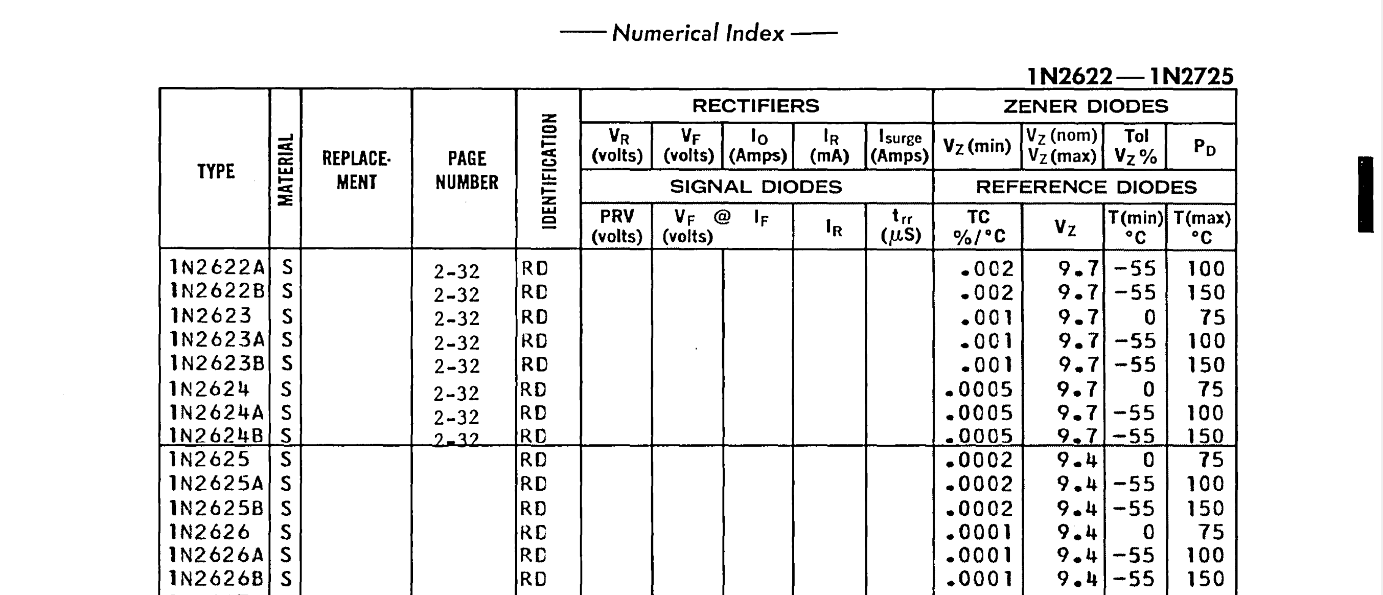
There are several zener diodes on the board, but only one of them has an elusive datasheet — the 1N2625. After combing through old semiconductor data books from the 1960s, I found some interesting information on this Zener diode in Motorola’s Semiconductor Data Book from 1966. This diode comes from a family of temperature compensated Zener diodes 1N262x. Ignoring temperature grades, there are three basic ones: 22, 23, and 24, which differ only in their temperature coefficient. But there are two more special ones in the series: 25 and 26, which sport even better TC values and have a slightly lower zener voltage of 9.4 vs 9.7 V.
If you try to track this part over the decades, it seems to have become / been rolled into the 1N937 series that, though obsolete, is still available from Microchip. But this 60 year old zener has a TC that is an order of magnitude better than its modern equivalent. This suggests that the 9.4 V reference voltage on this PCB plays a key role.
Best Guess
I see a precision voltage reference, what looks like a differential amplifier, and also know that the board was used in NASA test equipment. I immediately think “sensor interface card” — most certainly designed to interface with a strain gauge. A strain gauge is wired into one leg ( or more ) of a Wheatstone bridge excited by a precision voltage. The bridge imbalance is proportional to the strain of the material being measured. The weak signal is usually boosted by a differential amplifier followed by other conditioning circuits. And if your sensor interface card is flexible, you can also configure it to read RTDs, thermocouples, and other kinds of sensors as well. Sensor interface circuitry would certainly be a common need throughout NASA ground test equipment back in the 1960s, and today as well.
Excitation Driver
If my analysis is correct, the supply takes about +80 VDC on the input before all three zener voltage references become active. That seems a bit high. But back in the 60s, maybe this was a common B+ voltage. But, if you only supply say 28 VDC, transistors Q101 and Q102 bypass the top and bottom zeners. Maybe all that circuitry is there just to allow a wide range of input voltages?
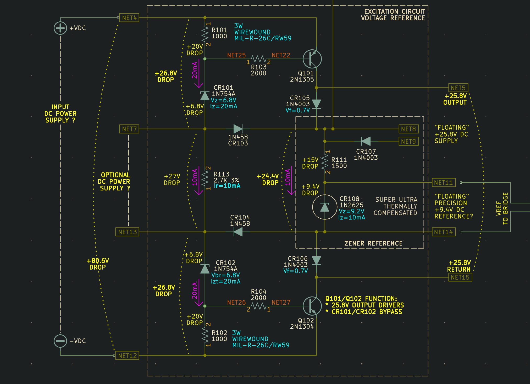
There seems to be a lot of unused edge connector signals, or at least signals I don’t understand, associated with this section. I have a nagging feeling that some of these might be used by other parts of the system to check that the interface card is present and working, and that the cables to the sensor have not shorted nor broken.
Differential Input Amplifier
On the Hackaday.io project discussion section, hacker [Lauri Pirttiaho] pointed out that four of the transistors appeared to make up a differential amplifier. He is right I believe, and if he got that by just glancing at the PCB photos, I’m really impressed. The circuit appears to drive a load located off-board, presumably generating a voltage to be recorded, plotted, converted to digital data, and/or viewed on meters. The operating point is biased by a current set by the zener and transistor combination CR109 / Q107, but the return path for that current isn’t clear. I guessed it returns through the output power supply return, as drawn on the schematics, but am not 100% confident.
This CR109 / Q107 bias circuit can be turned off by grounding edge connector signal NET17, thus disabling the difference amplifier output transistors. This could be a useful feature for multiplexing a group of sensors boards onto a single using A2D converter. Instrumentation quality A2D converters were probably more expensive back in 1962, so this seems like a reasonably guess.

Edge Connector, Nets
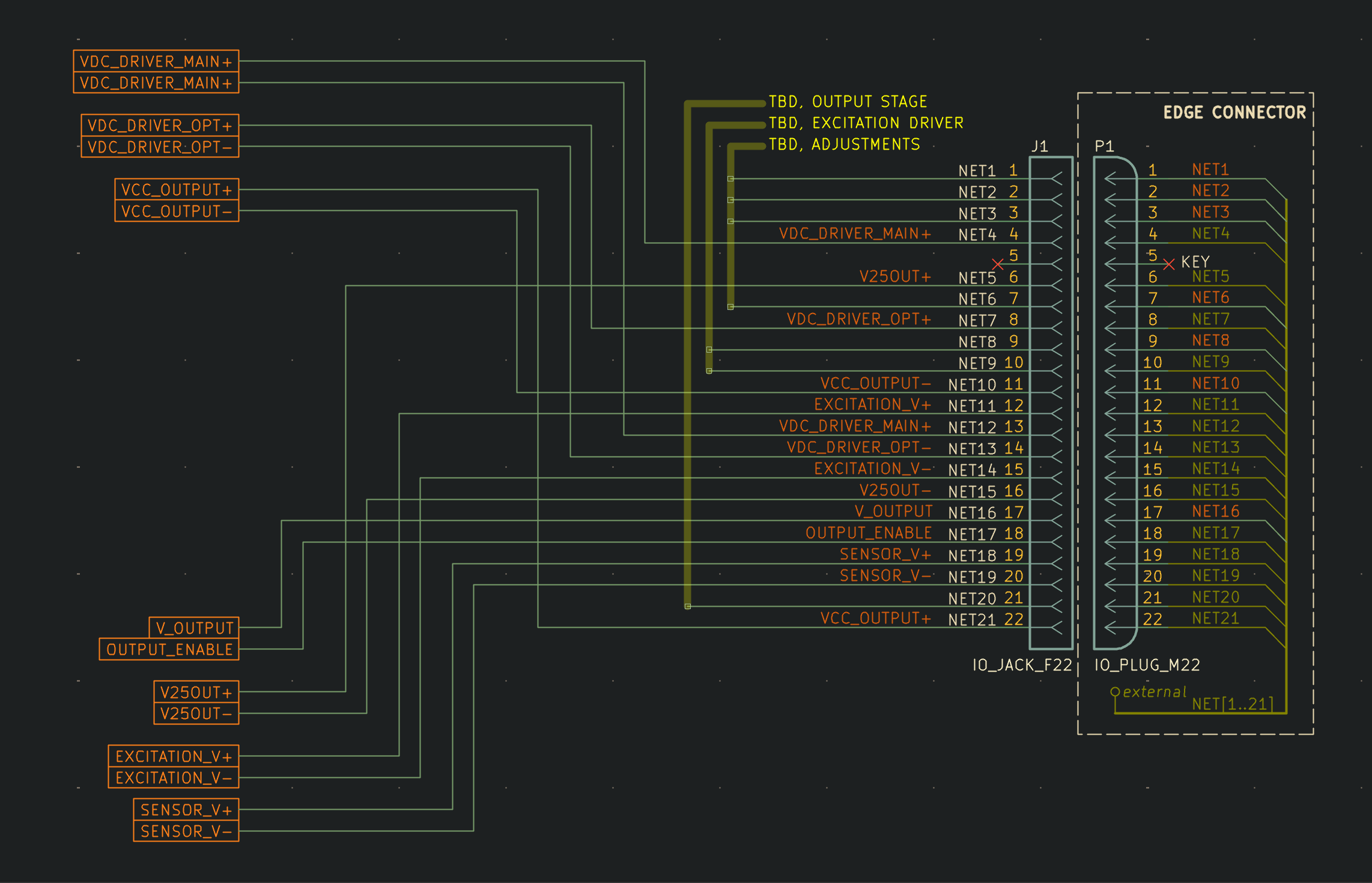
I connected the external signals up to a 22-pin edge-card connector schematic symbol and labeled them according to my guesses. The hope was that their positions along the card edge connector would give me additional insight. They did not. Lacking any descriptive names for the nets, [Skyhawkson] numbered them. I retained that same scheme here. Note that nets 1 through 21 are go to the card edge, and nets 22 through 36 are internal to the board. He numbered the net names sequentially along the card edge connector. But because of the keying gap in the connector, the net numbers don’t match the connector pin number from pin 5 onwards. For example, connector pin 6 is NET05 and so on.
Mystery Trimming
The section with the R125 current sense resistor also has a bunch of trimmer potentiometers, and almost all of the connections go off board. It might be use to adjust the gain and offset of the output signal. I also wonder these could somehow comprise the fixed legs of the bridge. I’m at a loss here.
Lessons Learned and Next Steps?
This KiCad reverse engineering project has been both easier and more difficult than previous ones. The PCB is so simple by today’s standards, and [Skyhawkson] has already done the tedious task of tracing out the connections. He’s also identified all the parts on the board and prepared a bill of materials. This was a great starting point.
In previous projects, I knew the schematic ahead of time or else I had a reasonable idea of the PCB’s functionality and flow of signals. In the case of this Apollo-era board, I knew nothing. It was just a bunch of transistors and supporting discrete components. It made me appreciate modern IC packages, where knowing a part number gives big clues about its function.
Hints can be found in even the simplest parts. Figuring out that diode 1N2625 was a zener with 0.0002 % temperature coefficient was a big clue that a precision voltage reference was present. The low value R125 is probably a current sensing resistor, but what current is being sensed is still not clear.
The redrawn schematics are found in this GitHub repository. If you have any further ideas about how this circuit board might have been used, please let us know in the comments below. If we get enough additional information, maybe [Skyhawkson] can be convinced to power up the board and test it out.



Seeing the conformal coating on the Title Photo brought back memories of broken components when I was repurposing those parts from excessed military circuits.
AIUI, the boards I used were from a decommissioned missile site.
Which KiCad theme is that?
Fiveseven, it is the Gruvbox theme. I believe I download it via the KiCad package manager. Looking at the KiCad forums, yes I did, this was added about two years back.
https://github.com/AlexanderBrevig/kicad-gruvbox-theme
I really like it because I’m using dark mode more and more (easier on the eyes). What I’m missing is an opposite color theme which is designed for printing. Say, a gruvbox-printer theme. I made the schematic images attached in this article by “printing” in color to a PDF. That looks great. But if I want a color hard copy or printable PDF, I don’t have a solution (other than using a ton of black ink/toner). I just print in black and white for now.
Thanks a lot!
For the printing issue, since 5.99 it has the option to not print the background color or just use an entirely different theme for the printout (e.g. a light one). Same for the Plot dialog.
Yeah. But that’s only half the problem. Colors that are high contrast against a dark background, like yellow, are almost indistinguishable against a white background. I’m thinking this is something that needs to be done artistically by a graphical designer or my some kind of opposite color transformation.
I see that the original VIM gruvbox color scheme has dark and light. Maybe gruvbox light would work well for printing.
That is more or less the point of the “opposite” color arrangements in newer light/dark themes from Solarized onwards. Not printing persay, but opposite contrast while retaining the same colors. Doing it programmatically isn’t straightforward btw, these relationships are not linear.
The best option would be for KiCAD themes to have dedicated print, which would essentially always be a “light” version of the theme with no background color. For now, Solarized Light works well for this out of the box.
S O. I came to that conclusion as well. Alas, Mr Brevig who made the Gruvbox for KiCad only made the dark theme. I’ll ping him and se how had did would be to mks RF might also.
Looked for “PC701” and found it might be a card used in Vidar Corp. Model 510 Integrating Digital Voltmeter, early 1960’s might be plexie, not even Nixie. Would have been a small fortune back then to make a DMM with no IC’s!
Another “PC701” I found as “Preamplifier Assembly” in Hoffer H01-1/2-550S turbine flow meter. Resoyurce:
https://nationalstocknumber.org/nsn/6680-01-151-3401
With mystery circuit boards, always search for any part numbers, silk text etc.
When reverse-engineering, I load the PCB comp and solder-side as layers into Gimp and then mirror the solder-side to make tracing it out easy.
Please excuse my naive attempt, but it wouldn’t have been for RF attenuation/impedance matching would it? Probably 99% chance I am completely wrong though lol
I’m pretty sure the part number is “107452-1” number stamped near the edge connector. Although that could be for the bare PCB I will admit. My attempts to find a reference to PC701 failed. I’ll dig some more into those possibilities, Kelly.
Love both doing and hearing about this kind of from-scratch electronics detective work! Reminds me of a signal conditioner card I looked at: https://www.eevblog.com/forum/projects/reverse-engineering-misc-avionics-(part-3-raytheon-eas-diehl)/msg5646971/#msg5646971
Some opinions and insights…
Mystery Trimming: R106 & R107 might be a coarse & fine adjustment for the same series resistance, looking at their values relative to the total series stack (esp. with R107 in parallel with a smaller resistor).
80V Input: I might be missing something, but I’m not sure why you marked 20 mA as going through CR101 & CR102? (and creating an extra total 40V through those 1K resistors) The 20V drop on each 1K doesn’t make sense, as it doesn’t account for the current that flows through the transistors; I think you might have the logic backwards on those or a misunderstanding of zener diode specifications. What it looks like to me is some kind of under-voltage lockout circuit:
* When CR101 & CR102 aren’t conducting (input voltage too low), the resistors pull Q101 & Q102’s Vbe to ~0V, and the transistors don’t conduct, and therefore no current flows to the middle section.
* But when the input voltage gets to 6.8V + ~0.7V on either side (min. 0.7 mA through each zener), this creates a large enough voltage drop on both 1K resistors to put a “normal” Vbe on Q101 & Q102, and both transistors turn on.
* The transistors, now active, pass current to and from the middle section directly.
This doesn’t really “bypass” the zeners though because there’s feedback: if Q101 conducts so much current or goes into saturation, for example, that Net8 got within 6.4V of Net4, then CR101 would stop conducting and Q101’s Vbe would drop to zero. So each zener + transistor combo keeps a minimum of ~7V between Net4-Net7 & Net13-Net12. Overall it should only need roughly 31V for the power supply.
My best guess is that the purpose of this section is to make sure that the Wheatstone bridge’s common-mode voltage sits far enough from either rail, that there’s headroom for the differential amplifier reading its output: no rail-to-rail op-amps here.
Good catch, Don. Those were my scribblings in the very beginning, kind of a first order analysis, where I was (incorrectly) ignoring Q101/Q102 entirely. Probably because at first, they made no sense to me with those extra card edge connections. What I was doing was looking at the specified test current of the 6.8V zener diode, which was 20 mA. And the specified zener current through the precision zener CR108 was 10 mA (that one is very important, to get at that low TC point). With all three zeners running at their rated currents, (and still ignoring Q101/Q102) you get a balanced. At the top, 20 mA flows through CR101 / R101, splitting into two paths: (1) 10 mA through R113 and (2) 10 mA through CR103, R111, CR108, and CR103. At the bottom, those currents combine again with 20 mA going through CR102 / R102. In this case, all the currents and voltages equal out. But yeah, we can’t ignore Q101/Q102. Good catch.
Ah yeah makes sense, figured it was probably something about the test current (really more of just a reference point). Either way, nice work, would be very happy to see more of this kind of article.
I wonder what this thing would look like made out of modern day surface mount components!
You know, they make DIP transistor arrays. I haven’t seen them as often these days, but I’m sure they make them in SMT variations, too. I’ve most recently used ones that were relay coil drivers, but you can get ones with signal transistors, also. Matched pairs, darlington, etc. Couple that with SMT resistors, you could make this pretty small, maybe 30 x 30 mm? But the limiting factor would be the power dissipation and the I/O connections rather than the parts.
Yesterday? I was doing inventory of a box of assorted ICs that I had bought at a yard sale a few years ago. I was was surprised to see that one compartment had some DIPs, instead of consisting of logic gates, were transistor circuits for analog signals. Yeah, I know, it could have been a 555!
B^)
I thought Nasa was famed for documentation ? In which case this circuit will be archived somewhere !
mikewhit, that’s a good point. But without a cage code (formerly FSCM) for the manufacturer, it might be a shot in the dark. And just because it was used at a NASA testing facility doesn’t necessarily mean it was an official NASA item. It could be from a time card stamping clock in the break room at a testing facility, as a silly example.
Man oh man. I wish I had the time to spend on such endeavors today. There was a time I bought Nasa surplus materials by the crate load direct from the Cape via the GSA Bidding program. This was in the 70’s and I made many a trip to the Cape after paying pennies a pound for truck loads of assorted electronics scrap that I later sold. I still have some Apollo era stuff but very little remains, as over 50 yrs have elapsed.
My first office mate was a former NASA engineer, and he told me of buying surplus piles of gear at auctions, and he would always make a profit by finding high value items which he could resell (and this was before eBay, and looking back, I’m pretty impressed he did this). I also remember he told me he built a home burglar alarm from space-qualified relays that cost hundreds of dollars new, but he got for pennies on the pound at auction.
So here’s a few thoughts.
First, Q105/106 are a long tail pair, with Q107/R124/CR109 being a constant current generator for the tail of around 3.8mA. NET17 will just likely just be a test point to monitor the reference diode. If you rearrange the schematic to show the pair this makes more sense.
The two outputs from this stage (Q105/106 collectors) drive the buffer/output stage Q103/104 with an output on NET16 as indicated. NET10 is almost certainly ground/0V. The really interesting point of this circuit is the gain resistor R118. I’ve not seen this exact configuration before, but my guess is that thus differential drive configuration both linearises the stage and improves its bandwidth (especially wrt 2nd harmonic distortion). If I can find time I may run a spice model on this for interest.
I only have the separate snippets of circuit here, but my first guess at the trimming resistors which also connect to the long tail pair input NET are that they are part of a Wheatstone bridge, which is probably what you were thinking too. I haven’t looked at exactly how this would connect though.
More on R118: thinking about the effect of this resistor, it is really quite a neat and clever configuration. If we assume that the whole circuit is in balance in its quiescent state, then the emitters of Q103 and Q104 will be at the same voltage, and so there is no current through R118. This means the quiescent BIAS currents through Q103/104 are essentially set by the long tail pair current, R120/121 and R114/115. All very straightforward and conventional. But, the GAIN through Q103/104 can be set independently by R118.