How small can an electric motor be without resorting to manufacturing methods like lithography? In a recent video, [Chronova Engineering] on YouTube tries to replicate the 1960 McLellan motor that fulfilled [Richard Feynman]’s challenge requirements. This challenge was part of [Feynman]’s 1959 lecture titled There’s Plenty of Room at the Bottom, on the possibilities of miniaturization. A $1,000 reward was offered for anyone who could build an electric motor that was no larger than 1/64th inch cubed (~0.0625 mm3), with the expectation that new manufacturing methods would be required to manufacture a motor this small.
As reported in the December 1960 issue of The Month at Caltech, [William McLellan] walked into [Feynman]’s lab with this tiny marvel that took him 2.5 months of lunch hour breaks to build. Weighing in at 250 micrograms and consisting out of 13 parts, it was constructed using a microscope, a watchmaker’s lathe and a toothpick. Surely replicating this feat would be easy today, right?
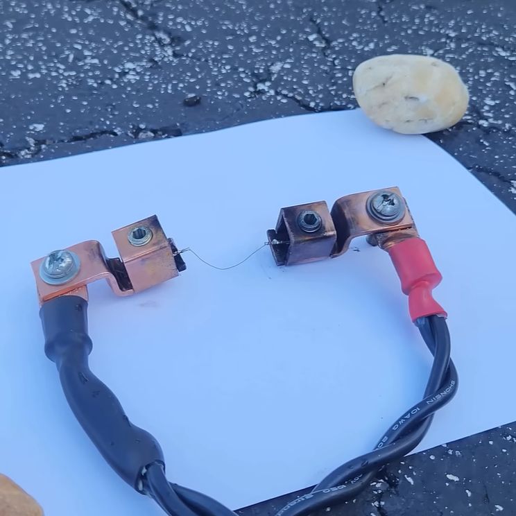
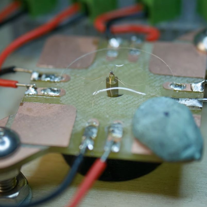
The main challenge is that everything is incredibly small. The rotor shaft is 90 micrometers in diameter, and the four coils require winding incredibly thin wire at scales where typical manufacturing methods do not apply. Suffice it to say that it takes massive amounts of patience, creativity and the best (stereo) microscope you can get, yet even with modern optics and materials this first attempt mostly failed.
At the end we’re left with SEM shots of this replication attempt and an immense amount of respect for the skills of [William McLellan] who made a working version in 1960 using much more basic tools during his lunch breaks.
Thanks to [J. Peterson] for the tip.
Continue reading “Building The Feynman Motor That Fits Through A Sewing Needle’s Eye”