The Guanella 1:1 balun. (Credit: Steve Arar)

Using Guanella Baluns As Impedance Transformers

Guanella Impedance Transformer. (Credit: FesZ Electronics)

Even before entering the mystical realms of UHF design, radio frequency (RF) circuits come with a whole range of fun design aspects as well. A case in point can be found in transmission line transformers, which are commonly used in RF power amplifiers, with the Guanella transformer (balun) being one example. Allowing balanced and unbalanced  (hence ‘balun’) systems to interface without issues, they’re both very simple and very complex. This type of transformer and its various uses is explained in a video by [FesZ Electronics], and also the subject of an article by [Dr. Steve Arar] as part of a larger series, the latter of which is recommended to start with you’re not familiar with RF circuitry.

Transmission line transformers are similar to regular transformers, except that the former relies on transmission line action to transfer energy rather than magnetic flux and provides no DC isolation. The Guanella balun transformer was originally described by Gustav Guanella in 1944. Beyond the 1:1 balun other configurations are also possible, which [Dr. Arar] describes in a follow-up article, and which are also covered in the [FesZ] video, alongside the explanation of another use of Guanella transformers: as an impedance transformer. This shows just how flexible transformers are once you can wrap your mind around the theory.

We have previously covered RF amplifier builds as well as some rather interesting balun hacks.

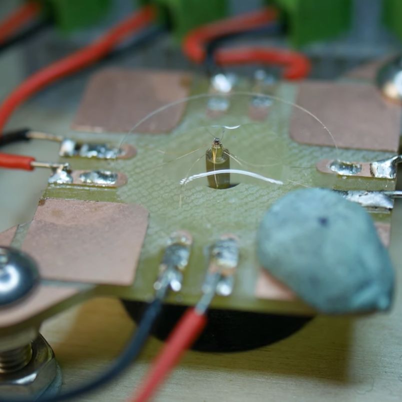
Heading image:  The Guanella 1:1 balun. (Credit: Steve Arar)

Continue reading “Using Guanella Baluns As Impedance Transformers”

Crystal structure of a monolayer of transition metal dichalcogenide.(Credit: 3113Ian, Wikimedia)

Transition-Metal Dichalcogenides: Super-Conducting, Super-Capacitor Semiconductors

Transition-metal dichalcogenides (TMDs) are the subject of an emerging field in semiconductor research, with these materials offering a range of useful properties that include not only semiconductor applications, but also in superconducting material research and in supercapacitors. A recent number of papers have been published on these latter two applications, with [Rui] et al. demonstrating superconductivity in (InSe2)xNbSe2. The superconducting transition occurred at 11.6 K with ambient pressure.

Two review papers on transition metal sulfide TMDs as supercapacitor electrodes were also recently published by [Mohammad Shariq] et al. and [Can Zhang] et al. showing it to be a highly promising material owing to strong redox properties. As usual there are plenty of challenges to bring something like TMDs from the laboratory to a production line, but TMDs (really TMD monolayers) have already seen structures like field effect transistors (FETs) made with them, and used in sensing applications.

TMDs consist of a transition-metal (M, e.g. molybdenum, tungsten) and a chalcogen atom (X, e.g. sulfur) in a monolayer with two X atoms (yellow in the above image) encapsulating a single M atom (black). Much like with other monolayers like graphene, molybdenene and goldene, it is this configuration that gives rise to unexpected properties. In the case of TMDs, some have a direct band gap, making them very suitable for transistors and perhaps most interestingly also for directly growing 3D semiconductor structures.

Heading image: Crystal structure of a monolayer of transition metal dichalcogenide.(Credit: 3113Ian, Wikimedia)

Google Open Sources PebbleOS: New Pebble Device In Development

The Pebble smartwatch was introduced in 2012 as part of a Kickstarter campaign and saw moderate success before the company behind it got bought out by Fitbit. Although a group of enthusiasts kept their Pebble devices alive, including via the alternate Rebble project for online services, it seemed that no new Pebble devices would grace this Earth. However, we now got a flurry of Pebble updates, with Google, the current owner of Fitbit, open sourcing the PebbleOS source, and [Eric Migicovsky] as the original Pebble founder announcing new Pebble watches.

These new Pebble watches would be very much like the original Pebble, though switching from a memory LCD to an e-paper screen but keeping compatibility with the original Pebble watch and its hackability. Currently there’s just a rePebble site where you can sign up for announcements. Over at the Rebble project people are understandably excited, with the PebbleOS source available on GitHub.

A lot of work still remains, of course. The Apache 2.0-licensed PebbleOS source was stripped of everything from fonts to the voice codec and Bluetooth stack, and of course bootstrapping whole new hardware production will require serious investment. Even so, for lovers of smart watches that work with modern-day smartphones, featuring an always-on display and amazing battery life the future has never been more bright.

Thanks to [Will0] for the tip.

New Open Source DeepSeek V3 Language Model Making Waves

In the world of large language models (LLMs) there tend to be relatively few upsets ever since OpenAI barged onto the scene with its transformer-based GPT models a few years ago, yet now it seems that Chinese company DeepSeek has upended the status quo. Its new DeepSeek-V3 model is not only open source, it also claims to have been trained for only a fraction of the effort required by competing models, while performing significantly better.

The full training of DeepSeek-V3’s 671B parameters is claimed to have only taken 2.788 M hours on NVidia H800 (Hopper-based) GPUs, which is almost a factor of ten less than others. Naturally this has the LLM industry somewhat up in a mild panic, but for those who are not investors in LLM companies or NVidia can partake in this new OSS model that has been released under the MIT license, along with the DeepSeek-R1 reasoning model.

Both of these models can be run locally, using both AMD and NVidia GPUs, as well as using the online APIs. If these models do indeed perform as efficiently as claimed, they stand to massively reduce the hardware and power required to not only train but also query LLMs.

Building The Feynman Motor That Fits Through A Sewing Needle’s Eye

The first attempt at replicating William McLellan's miniature motor. (Credit: Chronova Engineering, YouTube)
The first attempt at replicating William McLellan’s miniature motor. (Credit: Chronova Engineering, YouTube)

How small can an electric motor be without resorting to manufacturing methods like lithography? In a recent video, [Chronova Engineering] on YouTube tries to replicate the 1960 McLellan motor that fulfilled [Richard Feynman]’s challenge requirements. This challenge was part of [Feynman]’s 1959 lecture titled There’s Plenty of Room at the Bottom, on the possibilities of miniaturization. A $1,000 reward was offered for anyone who could build an electric motor that was no larger than 1/64th inch cubed (~0.0625 mm3), with the expectation that new manufacturing methods would be required to manufacture a motor this small.

As reported in the December 1960 issue of The Month at Caltech, [William McLellan] walked into [Feynman]’s lab with this tiny marvel that took him 2.5 months of lunch hour breaks to build. Weighing in at 250 micrograms and consisting out of 13 parts, it was constructed using a microscope, a watchmaker’s lathe and a toothpick. Surely replicating this feat would be easy today, right?

The main challenge is that everything is incredibly small. The rotor shaft is 90 micrometers in diameter, and the four coils require winding incredibly thin wire at scales where typical manufacturing methods do not apply. Suffice it to say that it takes massive amounts of patience, creativity and the best (stereo) microscope you can get, yet even with modern optics and materials this first attempt mostly failed.

At the end we’re left with SEM shots of this replication attempt and an immense amount of respect for the skills of [William McLellan] who made a working version in 1960 using much more basic tools during his lunch breaks.

Thanks to [J. Peterson] for the tip.

Continue reading “Building The Feynman Motor That Fits Through A Sewing Needle’s Eye”

Capacitor Decoupling Chaos, And Why You Should Abandon 100 NF

Everyone knows that the perfect capacitor to decouple the power rails around ICs is a 100 nF ceramic capacitor or equivalent, yet where does this ‘fact’ come from and is it even correct? These are the questions that [Graham] set out to answer once and for all. He starts with an in-depth exploration of the decoupling capacitor (and related) theory. [Graham] then dives into the way that power delivery is affected by the inherent resistance, capacitance, and inductance of traces. This is the problem that decoupling capacitors are supposed to solve.

Effectively, the decoupling capacitor provides a low-impedance path at high frequencies and a high-impedance path at low frequencies. Ideally, a larger value capacitor would be better, but since this is the real world and capacitors have ESL and ESR parameters, we get to look at impedance graphs. This is the part where we can see exactly what decoupling effect everyone’s favorite 100 nano-farad capacitors have, which as it turns out is pretty miserable.

Meanwhile, a 1 µF (ceramic) capacitor will have much better performance, as shown with impedance graphs for MLCC capacitors. As a rule of thumb, a single large decoupling capacitor is better, while two MLCC side-by-side can worsen noise. Naturally, one has to keep in mind that although ‘more capacity is better for decoupling’, there is still such a thing as ‘inrush current’ so don’t go too crazy with putting 1,000 µF decoupling capacitors everywhere.

Sony Ends Blu-Ray, MD And MiniDV Media Production

With the slow demise of physical media the past years, companies are gradually closing shop on producing everything from the physical media itself to their players and recorders. For Sony this seems to have now escalated to where it’ll be shuttering its recordable optical media storage operations, after more than 18 years of producing recordable Blu-ray discs. As noted by [Toms Hardware] this also includes minidisc (MD) media and MiniDV cassettes.

We previously reported on Sony ending the production of recordable Blu-ray media for consumers, which now seems to have expanded to Sony’s remaining storage media. It also raises the likelihood that Sony’s next game console (likely PlayStation 6) will not feature any optical drive at all as Blu-ray loses importance. While MiniDV likely was only interesting to those of us still lugging one of those MiniDV camcorders around, the loss of MD production may be felt quite strongly in the indie music scene, where MD is experiencing somewhat of a revival alongside cassette tapes and vinyl records.

Although it would appear that physical media is now effectively dead in favor of streaming services, it might be too soon to mark its demise.