After some water intrusion apparently killed one of [electronupdate]’s Amazon Blink Gen 3 cameras he took this opportunity to do a full teardown and analysis of all the major components. Spread across its three PCBs there are no fewer than two wireless ICs and a custom ASIC for all the major processing. There’s also a blog post with easy-to-ogle pictures.
The most basic PCB is effectively just a PCB antenna for the Silicon Labs EZR32 IC on the main PCB, using which the ~915 MHz connection with the central hub is maintained. The other smaller PCB is a bit surprising in that it contains a Cypress CYW43438 W-Fi b/g/n and BT 5.1 chip. This would seem to be used for the setup process, but considering that it also uses a central hub it is a bit of a mystery as to what it is used for exactly.
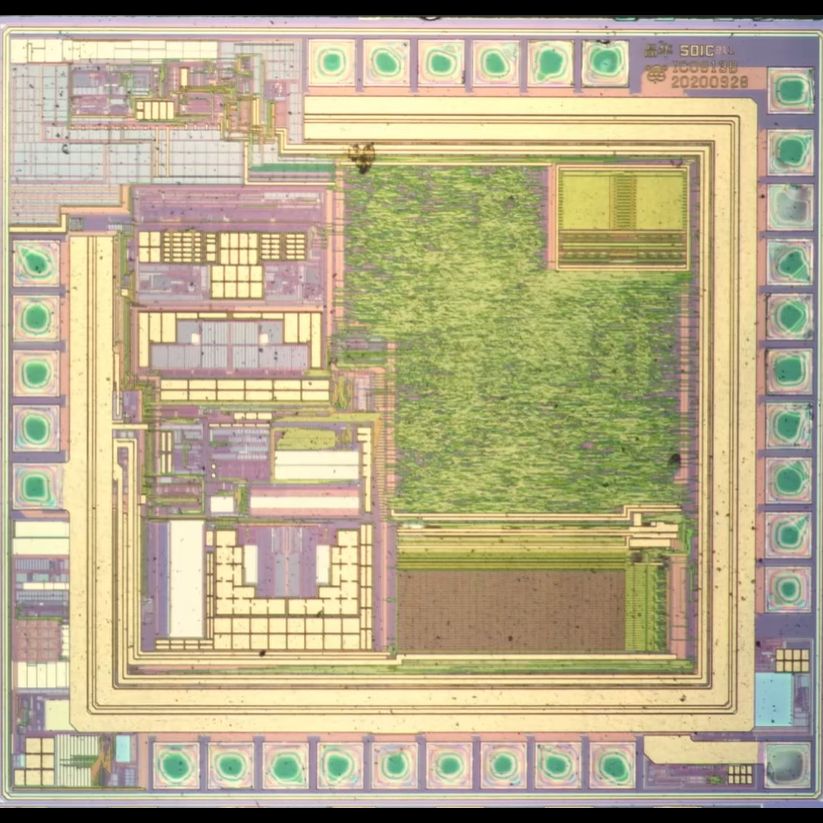
Finally, the main PCB contains all the major parts, with the custom Amazon Immedia ASIC that’s an integral part of this very low-power camera. Given that two AA cells being enough to run the camera for about two years, using off-the-shelf parts probably wasn’t good enough without some serious customization.
As for why this outdoors-rated camera failed after a few years in the outdoors, the reason appears to be water intrusion via the speaker opening. As for why a camera needs a speaker and not just the microphone is left as an exercise to the reader, but maybe it could be useful for yelling at the local kids to get off your darn lawn?
Continue reading “Reverse-Engineering An Amazon Blink Gen 3 Camera”