Some synthesizer sounds are just catchy, but some of them are genre-defining. We think you could make that case for the Roland JP-8000 patch “Sandstorm”, which you’ve heard if you listened to any trance from the 90’s, but especially the song that was named after it.
“Sandstorm” is powered by the Roland Supersaw, and synth nerds have argued for a decade about how it’s made. The JP-8000 is a digital synthesizer, though, so it’s just code, run through custom DSP chips. If you could reverse engineer these chips, make a virtual machine, and send them the right program, you could get the sound 100% right. Think MAME but for synthesizers.
That brings us to [giulioz]’s talk at the 39th Chaos Communication Congress, where he dives deep into the custom DSP chip at the heart of the JP-8000. He and his crew had approached older digital synths by decapping and mapping out the logic, as you often do in video game emulation. Here, getting the connections right turned out to be simply too daunting, so he found a simpler device that had a test mode that, combined with knowledge of the chip architecture, helped him to figure out the undocumented DSP chip’s instruction set.
After essentially recreating the datasheet from first principles for a custom chip, [guiloz] and team could finally answer the burning question: “how does the Supersaw work”? The horrifying answer, after all this effort, is that it’s exactly what you’d expect — seven sawtooth waves, slightly detuned, and layered over each other. Just what it sounds like.
The real end result is an emulation that’s every bit (tee-hee!) as good as the original, because it’s been checked out on a logic analyzer. But the real fun is the voyage. Go give the talk a watch.


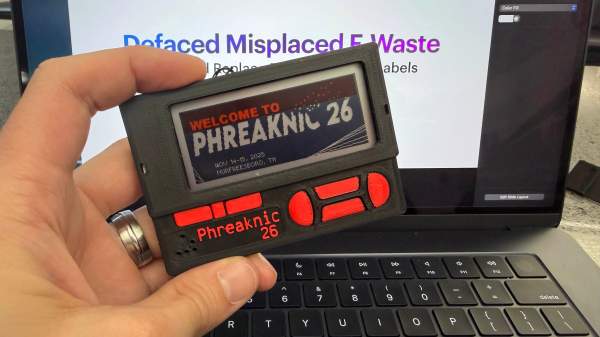
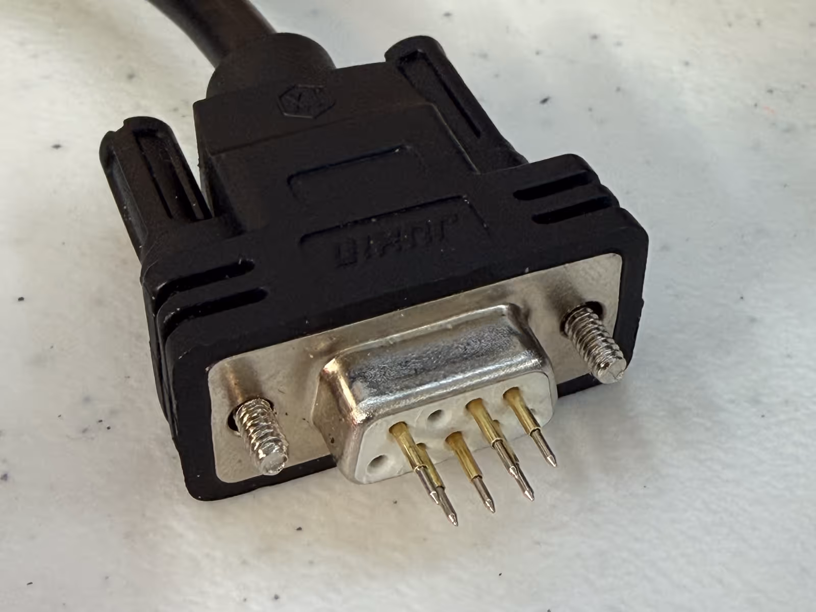 Another hacker assisting with the badge project, [Mog], noticed that the spacing of the programming pads on the PCB was very close to the spacing of a DB9/DE9 cable. This gave way to a very clever hack for programming the badges: putting pogo pins into a female connector. The other end of the cable was connected to a TI CC Debugger which was used to program the firmware on the displays. But along the way, even this part of the project got an upgrade with moving to an ESP32 for flashing firmware, allowing for firmware updates without a host computer.