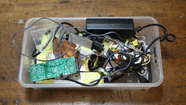
We love a good tear-down, and last week’s “Enginursday” at Sparkfun satisfied our desire to see the insides of AC-DC switching power supplies, accompanied by knowledgeable commentary. [MTaylor] walks us through how the basic circuit works and then points out why various other elaborations are made, and how corners are sometimes cut, in a few power supplies that he’s taken apart.
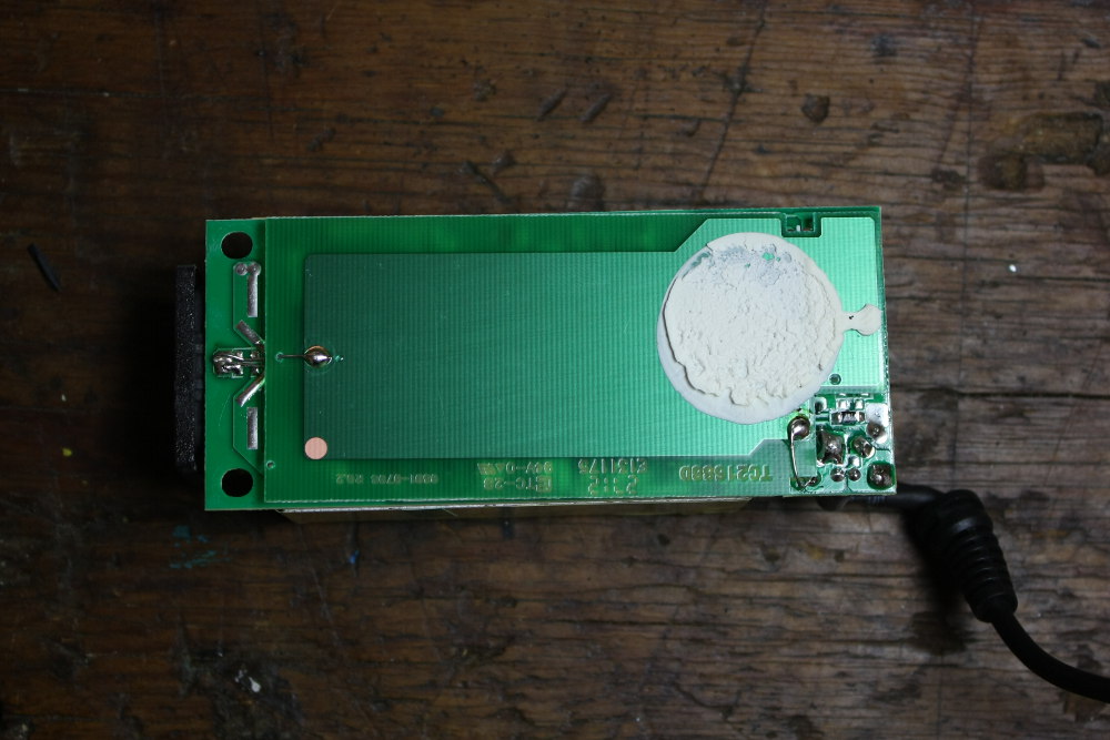 What struck us in the comparison was that some of the power supplies were very minimal designs, while others had “features” that were obviously added after the fact. For instance, the Li Shin supply (about half-way down the page) has an extra circuit board tacked on to the bottom of the real circuit board to act as EM shielding.
Rather than declare this a dodgy hack, as we would have, [MTaylor] declares it to be “Good News!” because it means that they’ve probably run an emissions test, failed it, and then added this bit on to make it pass. This is of course in contrast to the other makers who’ve probably never even considered emissions testing. Sigh.
If you’re interested in seeing more inner bits of power bricks, Sparkfun forum reader [sgrace] passed along this field guide to various power supplies, which is also worth a look. And if you’re interested in building yourself the ultimate bench power supply, look no further than this Hackaday.io project by [The Big One].

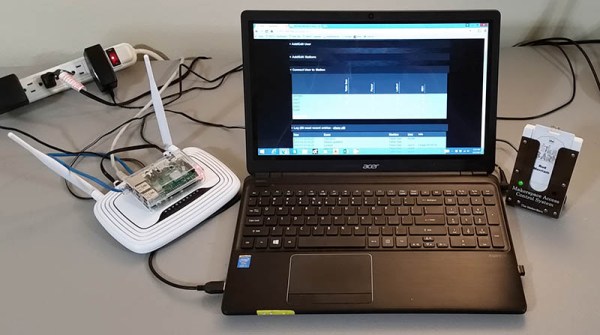
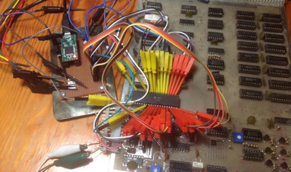
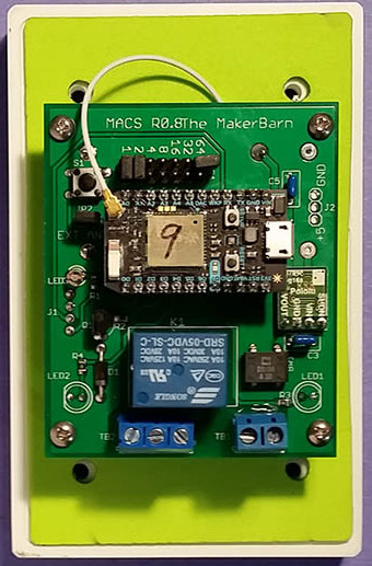 A control box, [George] calls them stations, controls the power to a machine. Member badges have an RFID tag that is read when inserted into the station’s reader. If the member is authorized to use the machine, the power is enabled. For safety, the member’s badge must remain in the reader to maintain power. The reader uses a Photon board from Particle with a WiFi link to a Raspberry Pi server.