 [x2jiggy] was given a non-functioning LCD monitor. He made a small effort to trouble-shoot its inability to display anything on the screen but couldn’t get it working again. When that failed he decided to repurpose it as light box instead of just sending it off for recycling.
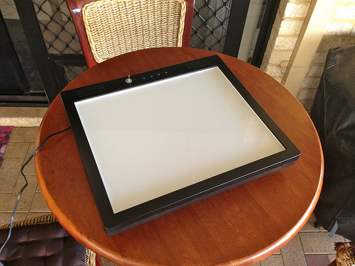
Monitor manufacturers put in a lot of effort to make sure the back lights distribute brightness as evenly as possible and that will make this a pretty good light box. [x2jiggy] starts off the conversion by removing the case. While it was off he gave it a new coat of paint. The LCD panel, the PCB that drives it, and the light diffuser sheets were all removed, leaving just the backlight and inverter PCB. A bit of probing with the multimeter and he even found a place to connect a toggle switch to actuate the inverter’s power. You can see the silver switch he added to the bezel in the image above. The full build video is embedded after the break.
Continue reading “Trashed LCD Monitor Turned Into A Light Box”