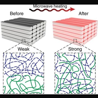
Layer adhesion is one of the weak points with FDM 3D printing, with annealing often recommended as a post-processing step. An interestingly creative method for this was published in Science Advances back in 2017, featuring the work of researchers at Texas A&M University and citing previous work by other teams. In the paper by [Charles B. Sweeney] et al, they describe how they coated PLA filament with carbon nanotubes (CNTs), resulting in this CNT being distributed primarily between the individual layers of polymer.
This is useful because CNTs are quite sensitive to microwave radiation, resulting in the conversion to thermal energy, i.e. heat. Compared to traditional annealing where the entire part is placed into an oven or similar, this microwave-based heating – or locally induced RF (LIRF) as they call this method – localizes the heat to the interface between two layers.
The advantages of this approach are that it doesn’t change the dimensions of the part noticeably, it’s faster and more efficient, and the annealing between layers approaches the strength of traditional manufacturing. Unfortunately not too much seems to have happened with this approach since then, but considering that both CNTs (single & double-walled) and microwaves are readily available, there’s not much standing in the way of replicating these results.


