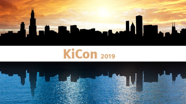
Oh, what’s KiCon you say? KiCon is the first dedicated conference on our favorite libre EDA tool: KiCad, organized by friend of Hackaday Chris Gammell and scheduled for April 26 and 27th in Chicago.
Having stuffed ourselves full of treats through the holidays, followed by sleeping through the calm winter months, we find ourselves once again facing the overwhelming tsunami of conference season. This year things are heating up early, and you’ll find a lot of Hackaday staff are headed to Chicago for KiCon.
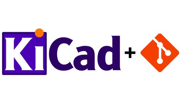
Now that early selection of talks has been released, the end of April can’t come soon enough. Being user focused the conference is centered around what people make using the tool, and how it can be leveraged to improve your next project. Wayne Stambaugh, the project lead for KiCad itself, will be on hand to talk about the state of the tool and what the road map looks like from here. There will be a pair of talks on effective version control and applying the practice of continuous integration and deployment to the EDA world. We’ll hear about methods for working with distributed project members and tips for designing easy to learn beginner soldering kits. And there will be two talks on RF and microwave design, one of which we hope will teach us how to use that mysterious toolbar with the squiggly lines.
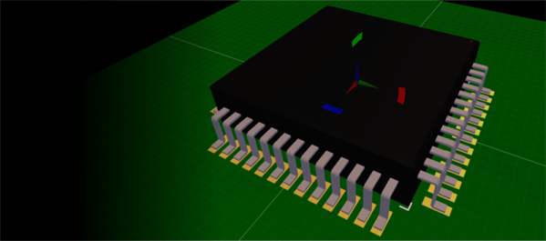
For an extra dash of flavor there will be a few Hackaday staff participating in the festivities. Anool Mahidharia is making the flight over to present a talk about how to quickly generate and use 3D models in FreeCAD, something we’re very interested in applying to our messy part libraries. Kerry Scharfglass will be around to walk through how to lay out a manufacturing line and design the test tools that sit on it. And our illustrious Editor in Chief Mike Szczys will be roaming the halls in search of excellent hacks to explore and brains to pick.
Interested in attending or volunteering for the conference? Now is the time to buy your tickets and/or apply as a volunteer!
Of course there’s a ton of fun and games that surround KiCon. Hackaday will be hosting another edition of our always exciting bring-a-hack the evening of Saturday April 27th after official activities wrap up. Plan to stop by and enjoy a beverage at this gathering of like minded hackers who are showing off awesome toys. We’ll get more location details out soon, but for now, grab a ticket to the con and make your travel arrangements.