Quick-Turn PCB Fab Hack Chat

Join us on Wednesday, July 31st at noon Pacific for the Quick-Turn PCB Fab Hack Chat with Mihir Shah!

We’ve all become used to designing a PCB and having it magically appear at our doorstep – after a fashion. Modern PCB fabs rely on economies of scale to deliver your design cheaply, at the expense of time – the time it takes to put enough orders onto a panel, and the time it takes to ship the finished boards from Far, Far Away.

Not everyone has that kind of time to burn, though. That’s where quick-turn fabs come in. These manufacturers specialize in getting boards to their customers as quickly as possible, helping them deal with sudden design changes or supporting specialty applications for customers.

It’s a niche industry, but an important one, and Royal Circuits is at the forefront. Mihir Shah is Director of Special Projects there, and he’s deep into the business of getting PCBs to customers as quickly as possible. He’ll drop by the Hack Chat to answer all your questions about how the quick-turn industry fits into the electronics manufacturing ecosystem, and to show off some of the tools of the future that they’re developing and investing in to streamline PCB design and analysis – from DebuggAR to PCBLayout.com, and more.

join-hack-chatOur Hack Chats are live community events in the Hackaday.io Hack Chat group messaging. This week we’ll be sitting down on Wednesday July 31 at 12:00 PM Pacific time. If time zones have got you down, we have a handy time zone converter.

Click that speech bubble to the right, and you’ll be taken directly to the Hack Chat group on Hackaday.io. You don’t have to wait until Wednesday; join whenever you want and you can see what the community is talking about.

DIY Tube Oven Brings The Heat To Homebrew Semiconductor Fab

Specialized processes require specialized tools and instruments, and processes don’t get much more specialized than the making of semiconductors. There’s a huge industry devoted to making the equipment needed for semiconductor fabrication plants, but most of it is fabulously expensive and out of reach to the home gamer. Besides, where’s the fun in buying when you can build your own fab lab stuff, like this DIY tube oven?

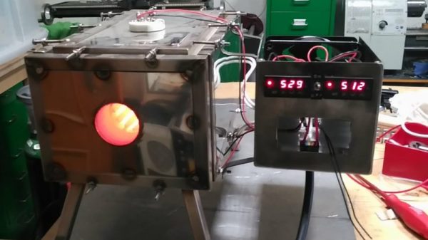
A tube oven isn’t much more complicated than it sounds — it’s just a tube that gets hot. Really, really hot — [Nixie] is shooting for 1,200 °C. Not just any materials will do for such an oven, of course, and this one is built out of blocks of fused alumina ceramic. The cavity for the tube was machined with a hole saw and a homebrew jig that keeps everything aligned; at first we wondered why he didn’t use his lathe, but then we realized that chucking a brittle block of ceramic would probably not end well. A smaller hole saw was used to make trenches for the Kanthal heating element and the whole thing was put in a custom stainless enclosure. A second post covers the control electronics and test runs up to 1,000°C, which ends up looking a little like the Eye of Sauron.

We’ve been following [Nixie]’s home semiconductor fab buildout for a while now, starting with a sputtering rig for thin-film deposition. It’s been interesting to watch the progress, and we’re eager to see where this all leads.

LED Fabrication From Wafer To Light

Building a circuit to blink an LED is the hardware world’s version of the venerable “Hello, world!” program — it teaches you the basics in a friendly, approachable way. And the blinky light project remains a valuable teaching tool right up through the hardware wizard level, provided you build your own LEDs first.

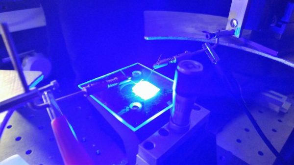
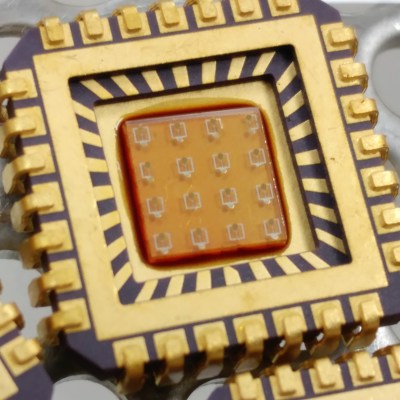
For [emach1ne], the DIY LED was part of a Master’s degree course and began with a slice of epitaxial wafer that goes through cleaning, annealing, and acid etching steps in preparation for photolithography. While gingerly handling some expensive masks, [emach1ne] got to use some really cool tools and processes — mask aligners, plasma etchers, and electron beam vapor deposition. [emach1ne] details every step that led to a nursery of baby LEDs on the wafer, each of which was tested. Working arrays were cut from the wafer and mounted in a lead frame, bonded with gold wires, and fiat lux.

The whole thing must have been a great experience in modern fab methods, and [emach1ne] should feel lucky to have access to tools like these. But if you think you can’t build your own semiconductor fab, we beg to differ.

[via r/engineering]

Graphene Grown On Semiconductors Big Step Toward Manufacturability

No modern technology has been met with more hype than graphene. These single-layer sheets of carbon promise everything from incredibly efficient power grids to more advanced electronics to literal elevators to space. Until now, though, researchers have yet to produce graphene sheets or ribbons in a reliable way. Researchers at the University of Wisconsin at Madison and the US Department of Energy Argonne National Laboratory have done just that, growing graphene nanoribbons on the surface of a germanium crystal.

By using a germanium crystal as a substrate, the researchers have found a directionality to the way these graphene nanoribbons form. This has been a problem for researchers experimenting with graphene microelectronics in the past; labs experimenting with making transistors out of carbon nanotubes found growth is highly unpredictable. The controlled growth of graphene nanoribbons opens the door to more precise fabrication, something that is necessary for microelectronics fabrication.

Synthesis of nanoribbons this small have not been possible before. Because germanium itself is a semiconductor – and was used for the first transistor – this discovery may pave the way for the creation of graphene-based circuits grown using the same semiconductor fabrication processes used today.

Fail Of The Week: Oil Expeller And Hasty PCB Layout

fotw-oil-extractor-hasty-pcb-layout

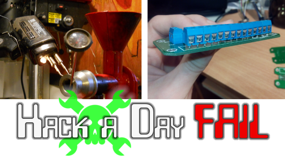
This Fail of the Week is a twofer. On the left we have an attempt to heat the output of an oil expeller. After a bountiful crop of sunflower seeds [Mark] picked up the oil expeller to make is own cooking oil. He tried to use the soldering gun as a heat source but after just a couple of minutes of on-time it melted the soldering iron’s plastic case. He’s looking for an alternate heat source but we wonder why he can’t just ditch the plastic and bolt this to a heat sink?

To the right is the product of hasty PCB layout. [Andrew] needed a USB to GPIO converter to use with his Android stick. He had built several of these before, etching the PCBs himself. But now he didn’t have the time to do his own etching and figured he could lay out a revision of the board and have it fabbed. Turns out this isn’t the time saver he had hoped. Problems with the location of silk screen labels aren’t a huge deal, but the ‘V’ in the board where his USB connector is located blocked any cable he tried to plug in. A bit of cutting solved that but he also had to deal with spring terminals whose leads wouldn’t fit the diameter of holes drilled in the board. We always print out the Gerbers and compare the footprints to our parts before submitting to the fab house. But we’re not sure we would have caught the USB cable clearance issue doing it that way. What checklists do you use before submitting your own boards?


2013-09-05-Hackaday-Fail-tips-tileFail of the Week is a Hackaday column which runs every Wednesday. Help keep the fun rolling by writing about your past failures and sending us a link to the story — or sending in links to fail write ups you find in your Internet travels.

[Ladyada’s] Thoughts On Quick-turn And Small-run PCB Houses

So you’ve mastered your PCB layout software, and it’s time to make the board. But if you don’t want to etch your own you’ve got to decided where to have it fabricated. There’s a slew of services out there, most of which you cannot afford, but the short list of those you can is still pretty long. We think this set of PCB fabrication house reviews will help you make your choice.

[Ladyada] — aka [Limor Fried] — knows what she’s talking about. She owns Adafruit Industries and has done the lion’s share of designing the many kits and items they sell. If you’re going to charge money for something it better work right, and that involves lots of prototypes. But even if you don’t need a quick turn-around or numerous testing boards the post is helpful as she also covers some of the batch producers we’re already familiar with. These include DorkBot PDX and BatchPCB to name a couple.

[via Reddit]

3d Printing Saves The Day For Time-lapse Photography

Several of us here at Hackaday have discussed how much we’d like to have some tools, like a 3d printer, but just can’t justify the cost. What would we make? Why do we really need one? Why don’t we just bother [Brian Benchoff] who already has one to make us parts instead. That’s usually how the conversation goes.

[Alexander Weber] gave us another little reason to drop in our “list of reasons we need a 3d printer” list with this little hack. He wanted to play with CHDK but found the camera’s battery unable to stay alive for longer than 2 hours. There is a commercially available adapter to allow you to plug into the wall, but the cost was outrageous. At least it is outrageous to someone who already owns a 3d printer. We just need a few hundred more dollars worth of reasons to justify that sweet 3d printer we’ve been pining over.

[via Adafruit]