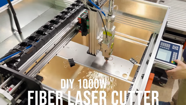
Sadly, the usual CO2-powered suspects in the DIY laser cutter market are woefully incapable of cutting metal. Sure, they’ll cut the heck out of plywood and acrylic, and most will do a decent job at engraving metal. But cutting through a sheet of steel or aluminum requires a step up to much more powerful fiber laser cutters. True, the costs of such machines can be daunting, but not daunting enough for [Travis Mitchell], who has undertaken a DIY fiber laser cutter build that really caught our eye.
Right off the bat, a couple of things are worth noting here. First — and this should be obvious from the fountains of white-hot sparks in the video below — laser cutters are dangerous, and you should really know what you’re doing before tackling such a build. Second, just because [Travis] was able to cut costs considerably compared to a commercial fiber laser cutter doesn’t mean this build was cheap in absolute terms — he reports dropping about $15,000 so far, with considerable ongoing costs to operate the thing.
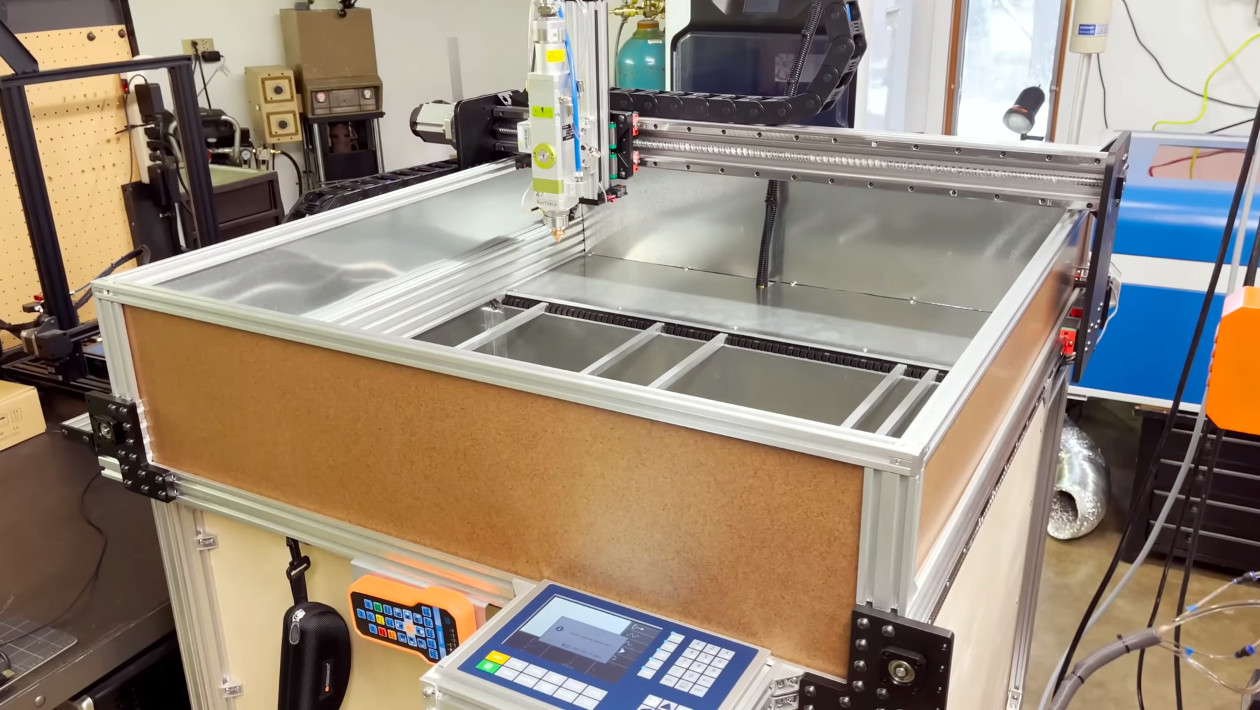
 That said, there doesn’t appear to be anything about this build that anyone with some experience building CNC machines wouldn’t be able to tackle. The CNC side of this is pretty straightforward, although we note that the gantry, servos, and controller seem especially robust.
The laser itself is an off-the-shelf machine, a Raycus RFL-C1000 fiber laser and head that packs a 1,000-Watt punch. There’s also the required cooling system for the laser, and of course there’s an exhaust system to get rid of the nasty fumes.
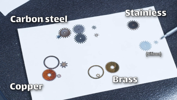
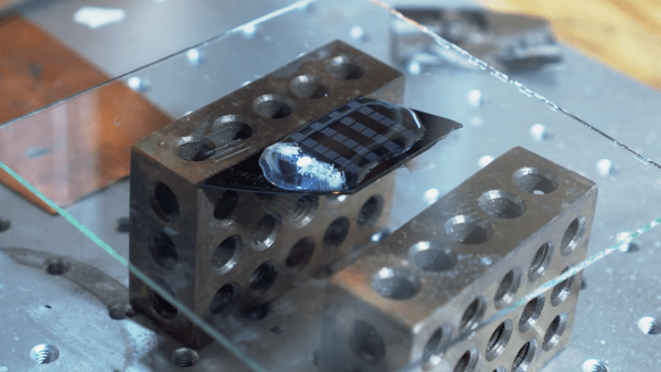
All that stuff requires a considerable investment, but we were surprised to learn how much the consumables cost. [Travis] opted for bottled gas for the cutter’s gas assist system — low-pressure oxygen for carbon steel and high-pressure nitrogen for everything else. Refills are really pricey, in part because of the purity required, but since the proper compressor for the job is out of the budget for now, the tanks will have to do. And really, the thing cuts like a dream. Check out the cutting speed and precision in the video below.
This is but the first in a series of videos that will detail the build, and if [Travis] thought this would whet our appetites for more, he was right. We really haven’t seen many DIY fiber laser builds, but we have seen a teardown of a 200-kW fiber laser that might tickle your fancy.
Continue reading “DIY Fiber Laser Adds Metal Cutting To The Mix” →